Tracking the trajectories of subatomic particles requires extremely precise detectors. As colliders achieve higher energies and experiments demand greater granularity, developers face growing challenges fitting all the sensing and processing electronics into compact, low-mass modules with high radiation tolerance. But an emerging technology promises a radical shift in detector design – opening new horizons for experimenters seeking to probe ever deeper into the quantum foundations of our universe.
This revolutionary approach involves stacking complete detector layers vertically using advanced interconnect techniques. Rather than spread electronics horizontally across silicon wafers, next-generation sensors will rise into the third dimension. 3D vertical integration provides routes to building lightweight, ultra-compact detectors with unprecedented performance, resolution, and radiation hardness. Mastering the third dimension opens new vistas for detector engineers, potentially enabling leaps in sensor technology to match coming leaps in collider capabilities.
The Promise and Challenges of 3D Vertical Scale Integration
What does shifting to three dimensional integration involve?
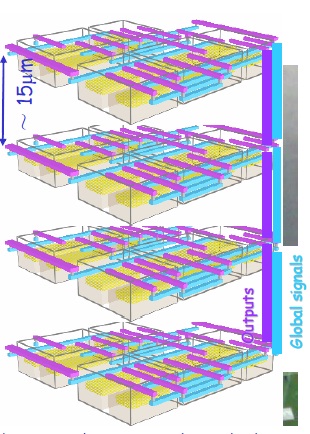
The key innovation is using advanced silicon vias (TSVs) and interconnect technologies to stack detector components vertically in separate tiers aligned precisely on top of one another [1]. This contrasts the traditional approach of packing electronics next to sensors across a single two-dimensional plane.
TSVs act as vertical “elevators” enabling signals to flow between tiers. This provides extensive flexibility optimizing each layer independently. One tier might contain the sensor matrix itself, customized for radiation detection. Another tier could hold analog front-end amplifiers and signal processing. A third tier might embed digital logic for control, calibration, and data transmission. Additional layers can incorporate power regulation, wiring, and shielding.
Attaching layers after independent processing avoids compromises or yield loss. Alignment precision under 5 microns enables integrating components at separate foundries into a heterogeneous stack. The modular encapsulation also promises to simplify manufacturing, testing, and assembly. Cost savings should scale with rising production automation.
Significant challenges remain to fulfill 3D integration’s promise across large scale detectors. These include refining TSV dimensions and densities, protecting sensitive elements from thermal stresses during bonding, lowering power demands through partitioning, and physics-driven co-simulation of complex heterogenous stacks. 3D integration also demands new thinking in systems engineering to properly leverage the extra dimension. But the VR/AR industry is helping drive rapid progress making vertical interconnect manufacturing practical.

Game-Changing Applications in Particle Tracking Detectors
What breakthrough detector capabilities might stacked 3D integration deliver?
Many transformative concepts require rethinking sensor architecture in three dimensions. Italian researchers recently proposed remarkable tracker designs integrating entire CMOS sensor planes vertically using TSVs [2]. This could enable single ultra-compact detector modules just micrometers thick directly measuring particles’ momenta from multiple position measurements across layers. The low material density minimizes troublesome scattering while retaining high resolution.
Other groups propose 3D integration to overcome challenges interfacing emerging sensor materials like graphene, GaAs, or diamond with processing circuits [3]. Stacked CMOS tiers would avoid compromising these sensitive media’s exceptional properties. Advanced sensors may also integrate processing elements vertically right inside each pixel cell. This promises order-of-magnitude leaps in channel density, speed, and radiation tolerance – crucial to sustain exabyte data rates in future collider experiments [4].
Detector engineers could also stack complete readout chips incorporating digitization, triggering, and network interfaces. Aligning thousands of TSV inputs precisely over sensor pixels enables marrying fine-pitch sensor arrays with proven CMOS electronics generations. Triply-redundant vertical integration might even provide a pathway to extremely reliable, self-healing sensor systems. And easy cartridge-like module swapping could simplify maintenance during long experimental runs.
Rising detector complexity strains testing capabilities. But vertical integration’s independent layers facilitate incremental qualification prior to final sensor integration. This also permits mixing complementary technologies like optical communications alongside high-density electronics. Detailed co-simulation of stacked heterogeneous components will help manage complexity creep by identifying interface risks early.
Conclusion: A Dimension of New Possibilities
3D vertical integration opens exciting new possibilities pushing sensor modules to extremes of performance, resolution, speed, reliability and radiation tolerance. Particle tracking detectors stand to achieve tremendous gains in capability by quite literally rising into the third dimension. Harnessing advanced interconnect techniques to build up rather than out promises to overcome looming barriers to realizing tomorrow’s transformative physics experiments.
Of course, the third dimension brings its challenges. But layer-by-layer verification provides a modular pathway to qualify ultra-complex stacks. And independent processing preserves each technology’s optimized functionality before integrating sensors, analogue electronics, digital logic, and communications interfaces into single compact detectors. By escaping planar constraints, 3D vertical interconnects offer particle experimenters extraordinary new degrees of freedom meeting demands anticipated in the coming decades. This extra dimension seems poised to drive a metamorphic leap for detector technologies – unleashing physics breakthroughs on the horizons of human knowledge.
References
- [1] P. Garrou, C. Bower and P. Ramm, Handbook of 3D Integration, Wiley-VCH, (2008).
- [2] D. Passeri, L. Servoli, S. Meroli, Analysis of 3D stacked fully functional CMOS Active Pixel Sensor detectors, JINST 4 (2009) P04009.
- [3] S. Lauxtermann, A. Zarandy, B. Czerny, 2.5D and 3D integration – a key enabler for heterogeneous micro-nano-bio systems, Proc. IEEE 103 (2015) 519-528.
- [4] M. Magera et al., Artificial retina in 3D stacked electronics, BioRxiv (2021).