
As traditional electronics face limits in Moore’s Law, Silicon Photonics steps in, using light to overcome these constraints and open new possibilities.
Silicon photonics is a technology that uses light to transmit and process information on tiny silicon chips. Just like how electronics use electrons to carry information, silicon photonics uses light particles called photons. These photons travel through thin channels called waveguides made of silicon, similar to the wires in electronic circuits. By controlling these light signals using various components like modulators and detectors, silicon photonics allows for super-fast data transfer and communication.
The advantages of silicon photonics include low-loss silicon waveguides, compact size, and mature CMOS processing. Modern packaging techniques have lowered costs and improved the scalability of silicon photonic integrated circuits (PICs), making them a viable solution for high-volume applications such as datacom and telecom.
Silicon photonics is poised to revolutionize the way we transmit and process data. It is already being used in a wide range of applications, and it is likely to become even more widespread in the years to come.
The Building Blocks of a Photonic Integrated Circuit
Silicon photonics leverages integrated photonic devices on cost-effective silicon substrates. Silicon enables low-loss waveguides linking diverse photonic elements culminating in functional Photonic Integrated Circuits (PICs).
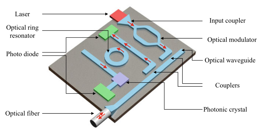
The PIC has different components that control and manipulate the light as it travels through it. The journey of light begins with a light source, often a laser, emitting focused and coherent light. This initial light signal serves as the foundation for subsequent processes.
As the light traverses the circuit, it follows carefully etched waveguides without significant loss, which act as pathways akin to optical fibres. Along this path, the light encounters modulators, devices capable of altering its properties. Modulators can change the light’s intensity, phase, or frequency, allowing information to be encoded onto the light signal. The manipulated light is then guided by the waveguides to couplers, which can either divide a single light signal into multiple paths or combine multiple signals into one path. Couplers facilitate the routing of light to different parts of the circuit for varied processing tasks.
Continuing its journey, the light interacts with filters, components that permit only specific wavelengths to pass through while blocking others. Filters play a pivotal role in applications such as wavelength division multiplexing (WDM), used in optical communication.
After being manipulated and processed, the light encounters photodetectors, devices that convert it back into electrical signals. When the light hits a photodetector, it generates an electrical current proportional to the intensity of the light. These photodetectors are essential for receiving and detecting light signals, forming a crucial link in the cycle of light manipulation. Finally, as the processed light completes its passage through the PIC, it reaches the output coupler, which guides the light out of the circuit in a controlled manner. This output coupler ensures that the modified light signal is prepared for further use, transmission, or interaction with other systems.
Why Silicon?
Silicon is a compelling candidate for silicon photonics due to its intrinsic material properties, advanced fabrication techniques, and seamless integration potential.
A key characteristic rendering silicon a prominent choice is its transparency within the crucial infrared wavelength range, aligning with prevalent optical communication bands. This optical transparency reduces signal loss, thereby enhancing the efficiency of data transmission and processing. Silicon’s transparency window extends from approximately 1.2 μm to 8 μm, including the near-infrared and mid-infrared regions where optical fibres exhibit minimal loss. This advantage leads to higher signal propagation distances and lower energy consumption, critical factors in high-speed data transmission scenarios.
Moreover, silicon’s compatibility with established complementary metal-oxide-semiconductor (CMOS) processes introduces the possibility of seamless integration with electronic circuits. With silicon’s thermal conductivity of approximately 148 W/m·K, it efficiently dissipates heat generated by photonic components, ensuring stable device operation under high data rates and reducing the need for complex thermal management systems.
Furthermore, silicon’s compatibility with modern lithography techniques facilitates the fabrication of intricate photonic structures with sub-micron precision. Additionally, silicon’s refractive index of approximately 3.45 at optical communication wavelengths ensures efficient light confinement within sub-micron waveguides, enabling compact device footprints.
In summary, silicon’s exceptional optical properties, compatibility with CMOS processes, advanced fabrication techniques, and established manufacturing infrastructure collectively position it as a formidable candidate for silicon photonics.
Advantages of Silicon Photonics over Traditional Technologies
Silicon photonics is a rapidly advancing technology that has several advantages over traditional technologies. One of the key advantages is its higher speed and bandwidth, which enables faster and more efficient data transfer.
Another advantage is the integration of photonics with electronics, which has been key to increasing the speed and aggregate bandwidth of silicon photonics-based assemblies. Additionally, silicon photonics has improved yield due to the development and fabrication of silicon photonics with modern, highly reproducible CMOS tools.
Finally, silicon photonics-based assemblies have lower power consumption than traditional technologies, making them more energy-efficient.
Main Limitations of Silicon Photonics
Despite its potential for high data transfer rates and miniaturization, silicon photonics has encountered challenges that warrant comprehensive scrutiny. One fundamental constraint lies in the quest for an efficient silicon-based light source, as crystalline silicon inherently lacks a direct bandgap, rendering the realization of monolithic silicon lasers elusive. This bottleneck prompts the reliance on external optical modules, complicating integration and potentially increasing energy consumption.
Additionally, their high refractive indices and submicron waveguide sizes contribute to intricate mode matching and mode conversion issues, impacting coupling efficiencies and overall device performance. The integration of silicon photonics with packaging and fibre coupling further poses intricate challenges, necessitating the development of efficient grating and edge couplers to mitigate reflection losses at the interface.
Further, the fabrication of photonic components, such as modulators and photodetectors, introduces process complexities that can impede device yield and reliability.
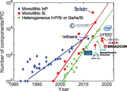
Industry Titans Shaping the Future of Silicon Photonics
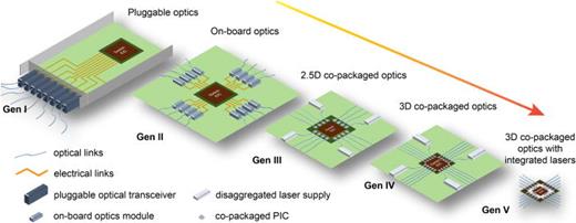
Significant advancements have been made by industry leaders like Broadcom, Intel, Cisco, and Hewlett-Packard Enterprise in enabling seamless integration of silicon photonics into existing communication systems. Silicon photonics has transformed the landscape of front panel pluggable transceivers, replacing discrete transceiver implementations with photonic chips that incorporate essential active and passive components.
Broadcom, for instance, has developed high-speed co-packaged switches, utilizing advanced switch ASIC SerDes to directly drive photonic integrated circuits. This approach eliminates the need for system-level re-timers and leverages the existing silicon packaging ecosystem, while also integrating BiCMOS electronics within a 2.5D stack for enhanced signal integrity.
Intel’s approach includes the integration of heterogeneous lasers onto photonic chiplets, showcasing high reliability and inherent design advantages. This approach ensures low failure rates, with redundancy mechanisms to counter single laser failure, resulting in robust and high-performance co-packaged switches.
Cisco has emerged as a major player in datacom and telecom with acquisitions of optical companies like Lightwire, Luxtera, and Acacia Communications. Their integration of CMOS opto-electronic Mach–Zehnder interferometers, germanium photodiodes, and various passive photonic elements within single silicon photonic PICs, combined with electronics integration, has paved the way for diverse data center interconnect applications.
Hewlett-Packard Enterprise has harnessed co-packaged optics for high-performance computing applications, employing DWDM solutions based on silicon photonics. Their platform incorporates robust quantum dot comb lasers, silicon microring modulators, and avalanche photodetectors, achieving a compact and energy-efficient DWDM interconnect for data rate scaling and power management in HPC environments.
Together, these industry giants exemplify the progress and impact of integrated silicon photonics, driving forward the development of advanced interconnect solutions that shape the future of communication systems.