The extremely hostile radiation environment where detectors operate requires a wide knowledge of radiation effects to assess the performance degradation of particle detectors induced by radiation damage.
The extremely fast reaction rate, as well as the beam-induced background, place strict requirements on the radiation hardness of the basic detector components. The tracking devices are subjected to high levels of harmful radiation and must maintain a minimum SNR for efficient particle detection. The primary effects of radiation damage can be divided into two categories: bulk damage and surface damage.
The former are typically caused by crystal atom displacement, whereas the latter include all effects in the covering dielectrics and the interface region.
On a macroscopic scale, damage in solid-state detectors causes:
- an increase of a leakage current translating into an increase in noise,
- a change in material resistivity,
- the reduction in the amount of collected charge due to the charge carrier trapping mechanism
- the decrease in the carrier’s mobility and lifetime.
As a result, the SNR decreases with increasing radiation damage. In terms of read-out electronics, it was discovered that radiation-induced surface effects at the Si-SiO2 interface, as well as defects in the bulk, cause the degradation of the parameters of bipolar and MOS devices. These effects are briefly summarised below.

Interaction of Particles with Matter: From Theory to Measurements
Understand the Mysteries of Radiation: Master the Interaction with Matter in a Few Simple Steps
Bulk Radiation Damage
Bulk damage is caused by the interaction of the incident particles with the nuclei of the lattice atoms. In contrast to ionization such interactions are not reversible in most cases. To remove a silicon atom from its lattice position a minimum recoil energy Ed of about 25 eV is required. Electrons need an energy of at least 260 keV to provide such a recoil energy in a collision, while protons and neutrons, because of their higher mass, require only 190 eV.
When only a small amount of energy is applied to the recoil Si atom, isolated displacements form, leaving a single vacancy-interstitial pair. They are primarily produced by low-energy electron and x-ray photon electromagnetic radiation.
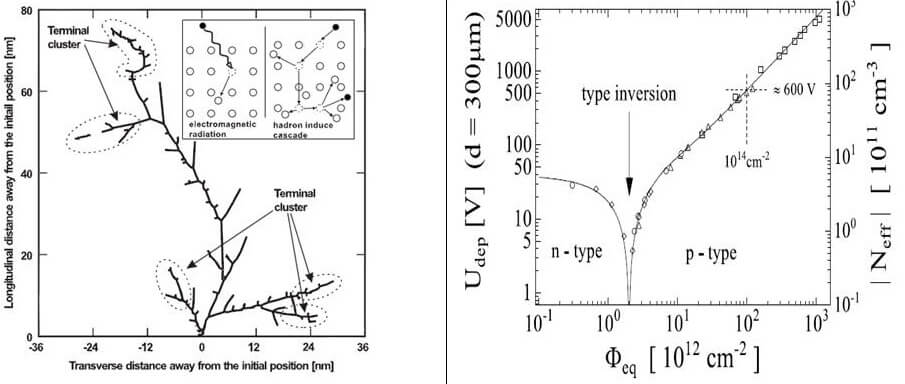
If the recoiling silicon atom receives enough energy from the collision, it may cause additional defects. To displace other Si atoms in the crystal and form a dense agglomeration of defects, a recoil Si atom requires approximately 5 keV of energy. Because these displacements are so close together, the majority of them can be repaired, and only 2% of all generated defects form electrically active states. These disordered areas are known as defect clusters. Defect clusters can be tens of nanometers wide and have a high local defect density. They have a greater impact on semiconductor device properties than point defects.
To be able to compare the damage caused by the different types of particles with different energies, radiation damage is scaled with the non-ionizing energy loss (NIEL). This quantity summarizes all energy deposited in the crystal which has not been used for the fully reversible process of ionization. The equivalent fluence of 1MeV neutrons is used as reference particles.
Both point defects and clusters can have severe effects on the detector performance, depending on their concentration, energy level and the respective electron and hole capture cross-section. Defects with deep energy levels in the middle of the forbidden gap could act as recombination/generation centres and are hence responsible for an increase in the reverse detector current. The dependence of the current per unit volume J can be parameterized as:
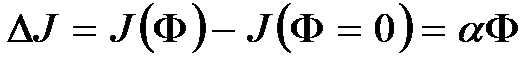
where α is the reverse current damage factor.
After irradiation, the leakage current anneals with time according to a process called annealing current which causes the cancellation of the damage into the lattice.
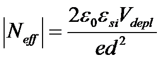
The removal of dopants by the formation of complex defects as well as the generation of charged centers changes the effective doping concentration Neff, which is the difference between all donor-like states and all acceptor-like states.
Neff can be determined from the full depletion voltage using:
The fluence dependence of effective doping and the full depletion voltage are plotted in Figure 1 (b). Starting with n-doped material it decreases up to a certain fluence of the order of Φ = (2–5)x10^12 cm−2 at which the space charge almost vanishes. With further irradiation, the absolute effective doping concentration increases again dominated by acceptor-like defects with a negative space charge. The depletion behaviour is now like in p-material.
Finally, these defects may act as trapping centres, reducing the efficiency of charge collection. The trapping is caused by the time constants of the electron capture and emission processes being different. Because there aren’t many free charge carriers in the depletion region, traps can hold or trap parts of the signal charge for longer than the charge collection time, lowering the signal height.
For most of the tracking devices used in particle physics, this effect is much less of a problem than the other radiation-induced effects already mentioned. After a fluence of 10^14 neq/cm2 about 90% of the generated charge in a 300 μm thick detector can be collected.
However, this number decreases to about 50% for 10^15 neq/cm2 and trapping will eventually limit the use of silicon detectors for fluences much beyond this number. In spectroscopic applications trapping causes serious degradation as it affects the pulse height. Devices exposed to radiation, like satellite-based X-ray telescopes, have to be frequently recalibrated to take into account the effects of radiation-induced trapping centres.
Surface Radiation Damage
In silicon, the surface region is also sensitive to radiation. The term surface damage summarizes all defects in the overlaid dielectrics, e.g. the silicon oxide, and the interface between the silicon and the dielectric. As the crystal structure of silicon oxide is highly irregular, displacements of single atoms due to irradiation do not lead to macroscopic changes.
Ionization in the oxide, however, is not fully reversible and may cause steady changes in the interface properties. After the creation of electron–hole pairs in the oxide layer, most electron–hole pairs recombine immediately. As electrons have high mobility in the oxide (μn,oxide ≈ 20 cm2/(Vs)) they will be collected by any positively biased electrode close by.
The holes have very low mobility in the oxide instead (μp,oxide ≈ 2×10^(−5) cm2/(Vs)) because of a large number of shallow hole traps. They move very slowly in the direction of the electric field in the oxide, hopping from one shallow trap into the next. If the holes arrive in the transition region between silicon and oxide, where many deep hole traps exist, they may be kept there permanently.
These charges which are now fixed represent an additional contribution to the total oxide charge Nox, which leads to an increase in the capacitive coupling between pixels. Direct consequences are the greater charge collection sharing between pixels and an increasing noise due to the rise of the capacitive load seen by the electronic readout.
Some parts of the stuck holes, i.e. those that are closest to the interface, may recombine with electrons coming from silicon. The electrons reach the oxide volume by the tunnel effect which reduces the amount of positive charge trapped in the oxide. The probability of tunnelling electron jump increases exponentially with decreasing thickness of the concerned oxide volume. Thus, the thin oxide of a deep sub-micrometre MOS transistor is intrinsically more radiation tolerant than thicker oxides used in past technologies.
For gate oxide thicknesses above approximately 20 nm, the shift of threshold voltage after irradiation ΔVth is proportional to the squared value of the oxide thickness ΔVth –> tox^2. On the other hand, the threshold voltage shift below 20 nm decreases even faster approaching the dependence ΔVth –> tox^3 at the corresponding irradiation dose.
Standard bulk CMOS processes use p-type substrate wafers, and accumulated positive charges may provoke short circuits in the design. The effect is strongly enhanced under thick oxide regions, where leakage currents appear close to the interface. Shallow surface channels can be created between different n-type regions implanted on the chip if they are separated only by lightly doped p-type silicon. Moreover, the charge accumulated at the ends of polysilicon gates designed in a classical rectangular form of NMOS transistors may prevent them from being switched off completely.
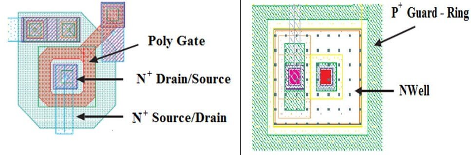
This is why, the use of enclosed NMOS transistor gates and p+-type guard rings of increased doping were introduced for wide use. Complying with this design rule makes radiation-hard electronics possible using standard inherently radiation-soft processes. This is commonly used now for radiation-hardened read-out circuits designed for high-energy physics experiments.
Figure 2 (a) shows the principle of the radiation tolerant layout of an NMOS transistor with an enclosed polysilicon gate and the use of a p+-type guard ring protecting against leakage currents between n-type regions in the design (Figure 2 (b) ).
At any Si-SiO2 interface, there are numerous interface traps, which result from the strained or dangling silicon bonds at the boundary between the two materials. The density of the interface traps depends strongly on the processing parameters, such as oxidation temperature, and is usually in the range from 10^9 cm-2 to 10^10 cm-2.
Ionizing radiation causes the density of these traps to increase and modifies their energy distribution, giving rise to radiation-induced interface traps, hence new energy levels are introduced in the band gap at the Si-SiO2 interface. They play the role of additional acceptor or donor states, which under thermal equilibrium are charged. Trapped charges alter the electrical characteristics of the devices by modifying the electric fields inside. The energy levels close to the mid-gap may act as trapping centres for charge carriers generated by incident particles in the detector.
This effect is observed as partial charge collection after irradiation. The charge carriers generated by an incident particle are blocked in trapping centres and are released with some delay after the particle passage. The increased density of energy states in the band gap, which can act also as generation-recombination centres, increases the recombination velocity at interfaces. This effect translates primarily into an increased leakage current. For some detectors, the generation at the Si-SiO2 interface is the dominant source of a dark current.
Read-out circuits suffer from the effect of positive charge build-up, the decreased carrier’s surface mobility and the high density of interface states with energy levels in the band gap. Due to the creation of new interface traps, both NMOS and PMOS transistors, suffer from the increase of absolute value of their threshold voltages. The increased density of the interface states has also an impact on the flicker noise of the NMOS transistor whose level is significantly higher compared to the PMOS device and is further deteriorated after irradiation.
References
- M. Moll Phd Thesis Radiation Damage in Silicon Particle Detectors
- Techniques for Nuclear and Particle Physics Experiments by W. R. Leo
- I.M.Bronshtein, B.S. Fraiman, “Determination of the Path Lengths of Slow Secondary Electrons”, Sov. Phys. Solid State, Vol.3, (1961), pp.1188-1197
- R. Wunstorf, Systematische Untersuchungen zur Strahlenresistenz von Silizium-Detektoren fur die Verwendung in Hochenergiephysik-Experimenten, PhD Thesis, Universitat Hamburg, Germany (1992)
- G.Anelli, et al., Radiation Tolerant VLSI Circuits in Standard Deep Submicron CMOS Technologies for the LHC Experiments: Practical Design Aspects, IEEE Trans. Nucl. Sci., Vol.46, No.6, (1999), pp.1690-1696