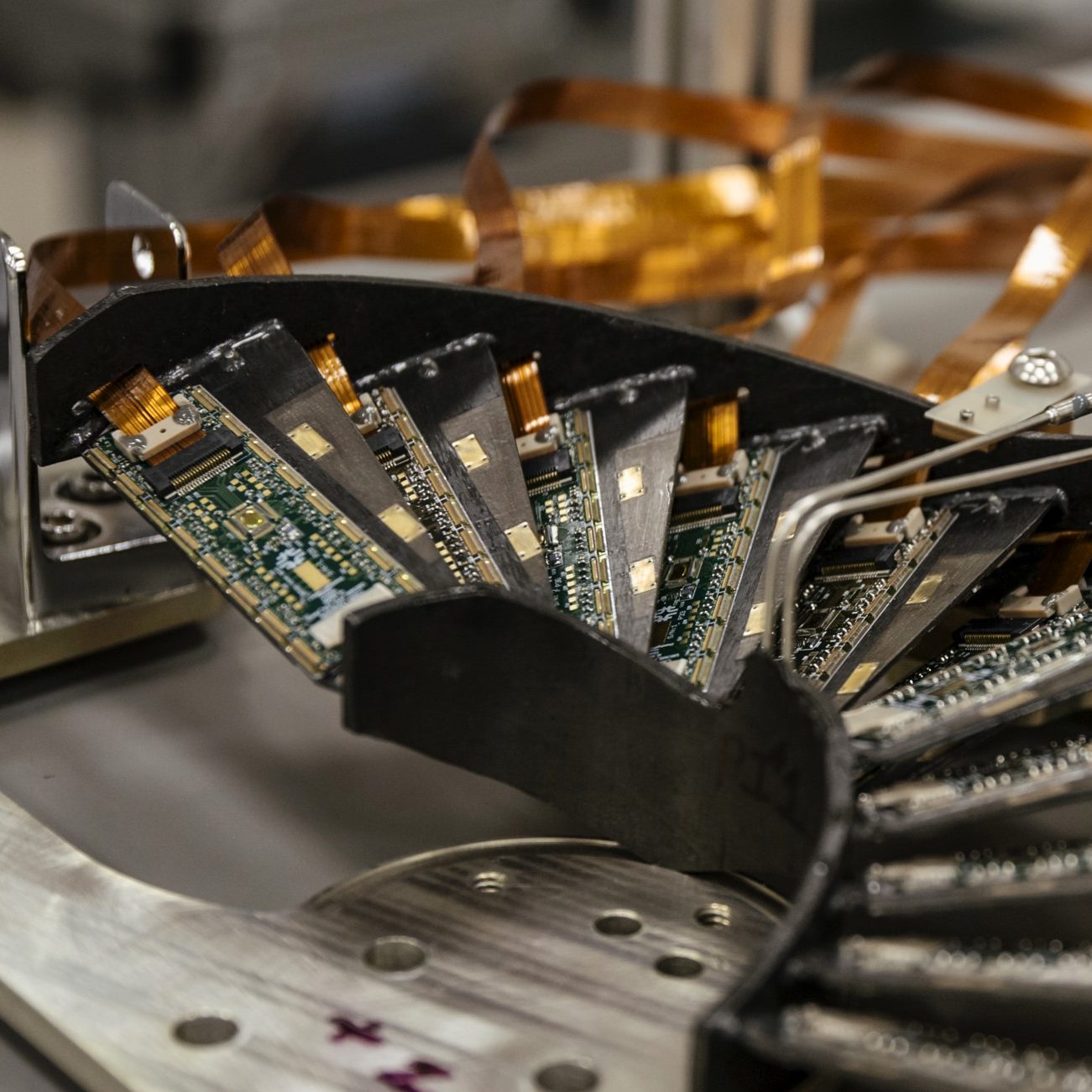
Silicon sensors have revolutionized particle physics over the past four decades, providing unmatched spatial precision and rate capabilities. As we look toward the future of high-energy physics with upgraded facilities and new colliders on the horizon, silicon detector technology continues to evolve at a remarkable pace. This evolution is driven by increasingly challenging experimental requirements, from higher radiation tolerance to unprecedented timing precision. This article explores the cutting-edge developments in silicon detector technology and their promising future in particle physics experiments.
The Silicon Revolution in Particle Physics
Silicon has become the dominant semiconductor material for position-sensitive detectors in particle physics, and for good reason. Its moderate band gap of 1.12 eV is large compared to room temperature thermal energy (25.9 meV), eliminating the need for cooling except in ultra-low noise applications or to mitigate radiation damage. Silicon detectors detect particles through ionization, creating electron-hole pairs that produce electrical signals. With an energy requirement of just 3.6 eV to create an electron-hole pair, silicon yields approximately 80 electron-hole pairs per micrometer, allowing for relatively thin detectors compared to gaseous alternatives.
Since their introduction in the 1980s, silicon-based tracking detectors have revolutionized high-energy physics (HEP) experiments with their unmatched spatial resolution and high-rate capabilities. Their sensitive areas have grown remarkably, increasing by an order of magnitude each decade – from 1 m² (vertex detectors at LEP) to 10 m² (CDF) to 200 m² (CMS Tracker) to 600 m² (CMS High Granularity Calorimeter). This progression reflects both technological advancement and the expanding role of silicon detectors in modern particle physics.
Current Limitations Driving Innovation
Despite their success, conventional silicon sensors face significant challenges. Current position resolution for single particle hits remains larger than a few microns, a limit reached over 30 years ago. The minimum ionizing path length that sensors can detect is several tens of microns, making them unsuitable for applications requiring detection of short recoiling atom paths. These limitations stem from fundamental aspects of current technology and are unlikely to be overcome through mere refinements of existing designs.
Perhaps the most pressing challenge is radiation damage. As accelerators become more powerful and detectors are placed closer to interaction points to maximize data collection, silicon sensors face increasingly intense radiation levels. For example, inner pixel detectors at the High Luminosity LHC (HL-LHC) will need to withstand approximately 10¹⁶ highly damaging particles per cm² and doses approaching 10 MGy. These extreme conditions severely impact detector performance and longevity.
Emerging Silicon Sensor Technologies
From Planar to 3D Silicon Sensors
One of the most significant innovations in silicon detector technology is the development of 3D silicon sensors. Unlike conventional planar sensors, 3D sensors feature columnar electrodes that penetrate through the silicon bulk, reducing the collection distance while maintaining sensor thickness. This architecture offers superior radiation tolerance, making 3D sensors excellent candidates for the innermost parts of tracking systems in high-radiation environments.
Recent studies have demonstrated that 3D pixel sensors with 50 × 50 μm² pixel size can maintain average efficiencies above 96% even after exposure to fluences of 1 × 10¹⁶ neq/cm² when biased to 80 V. This exceptional radiation hardness has led to their adoption in the ATLAS Inner Tracker upgrade for the HL-LHC.
Low Gain Avalanche Diodes (LGAD)
Low Gain Avalanche Diodes (LGAD) represent another breakthrough in silicon detector technology. LGADs feature a gain layer between P and N++ regions that provides internal charge amplification with gains of 10-50, significantly improving signal-to-noise ratios while maintaining fast timing. This innovation has enabled timing resolutions of less than 35 ps, making LGADs ideal for applications requiring precise time measurement.
The LGAD technology has been chosen for the ATLAS High Granularity Timing Detector (HGTD) and CMS Endcap Timing Layer (ETL), both of which will begin data collection around 2028. These detectors will provide precise timing information to help disentangle overlapping events in the high-pileup environment of the HL-LHC.
AC-coupled LGAD (AC-LGAD)
Building on LGAD technology, AC-coupled LGAD (AC-LGAD) sensors offer further improvements in position resolution while maintaining excellent timing performance. In AC-LGADs, electrical signals in a resistive but continuous n+ layer are AC-coupled to metal electrodes. This design provides 100% fill factor (active area) and much better spatial resolution due to signal sharing between metal electrodes.
Recent tests have demonstrated spatial resolutions of approximately 20 μm (20-30 times smaller than the electrode pitch) with timing resolutions of around 30 ps simultaneously. This remarkable performance makes AC-LGADs strong candidates for 4D trackers in future high-energy experiments.
Depleted Monolithic Active Pixel Sensors (DMAPS)
Depleted Monolithic Active Pixel Sensors (DMAPS) integrate sensor and readout electronics on the same substrate, offering significant advantages in terms of material budget and cost compared to hybrid designs. Modern DMAPS prototypes utilize high-resistivity substrates and apply high bias voltages to deplete the sensing volume, enabling fast charge collection through drift rather than diffusion.
For example, the LF-Monopix prototype, manufactured in LFoundry 150 nm CMOS technology on a high-resistivity P-type wafer, demonstrates the potential of DMAPS for high-rate environments. By encapsulating all pixel electronics within the charge collection electrode, these sensors achieve a large fill factor, potentially improving radiation hardness.
Resistive AC-coupled Silicon Detector (RSD)
The Resistive AC-coupled Silicon Detector (RSD) represents another novel approach for enabling 4D tracking. RSD sensors utilize a gain implant similar to LGADs, but segmentation into pixels is provided by AC-coupled electrodes, enabling high spatial resolution through charge sharing. The key to controlling charge sharing is a precisely tuned n+ resistive layer, which differs from the standard LGAD’s highly conductive n++ layer.
RSDs allow for precise position resolution while providing a 100% fill factor and requiring fewer readout channels than traditional pixel sensors, potentially reducing system complexity and cost.
The Quest for 4D Tracking
Perhaps the most transformative trend in silicon detector development is the pursuit of “4D tracking” – the ability to measure both the spatial coordinates and arrival time of particles with high precision. This capability would revolutionize particle physics experiments by enabling time-of-flight measurements and significantly reducing track reconstruction ambiguities in high-occupancy environments.
Achieving effective 4D tracking requires silicon sensors with both excellent spatial resolution (microns or better) and timing resolution (tens of picoseconds). This combination is driving the development of new sensor architectures like AC-LGADs and monolithic LGADs, which promise to deliver both capabilities in a single, cost-effective silicon tracker.
As an example, the Silicon Tracking System (STS) for the CBM experiment achieves timing resolution of approximately 5 ns while providing precise spatial measurements, using Double-Sided Double Metal (DSDM) silicon microstrip sensors with a material budget of just 2%-7% X₀. This demonstrates the feasibility of low-mass 4D tracking systems, a critical consideration for future detector designs.
Applications in Future Colliders
The requirements for silicon trackers at future facilities are driving sensor innovation toward new extremes. Future lepton colliders (CEPC, FCC-ee, ILC, CLIC) and hadron colliders (FCC-hh) will demand unprecedented performance from tracking detectors.
For instance, the proposed Circular Electron Positron Collider (CEPC) is exploring the use of strip-type AC-LGADs for its outer silicon tracker, with ambitious goals for spatial resolution (10 μm) and timing resolution (50 ps). Similarly, the Future Circular Collider (FCC-hh) will require detectors capable of reconstructing and identifying particles with momenta as large as 20 TeV, operating optimally across a wide energy spectrum.
These future colliders will benefit from “Monolithic LGAD” sensors, which integrate LGAD sensor elements with readout electronics on the same substrate. Such devices could potentially transform MAPS detectors’ timing information from typical values of ~10 ns to ~50 ps, enabling true 4D measurements in a single, cost-effective silicon tracker.
Collaborative R&D Efforts
The advancement of silicon sensor technology relies heavily on collaborative research and development (R&D) efforts. The RD2, RD48, and RD50 collaborations spearheaded groundbreaking advancements in radiation-tolerant silicon detectors. These efforts led to significant innovations, such as the development of Diffusion Oxygenated FZ (DOFZ) silicon with high oxygen content, which exhibited improved resistance to radiation damage from charged hadrons.
More recently, the DRD3 collaboration has taken up the mantle, aiming to continue this success while extending the scope to monolithic CMOS pixel sensors and 3D integration. DRD3 serves the dual purpose of promoting strategic developments outlined in the detector R&D roadmap while encouraging innovative “blue-sky” research in solid-state detectors.
Other significant R&D initiatives focus on specific technologies, such as the TANGERINE project developing monolithic active pixel sensors in 65 nm CMOS imaging process, and various institutional efforts to advance AC-LGAD technology for 4D tracking applications.
Toward a New Generation of Detectors
The ultimate goal of current silicon sensor R&D is to enable detectors with sub-micron spatial resolution – on the order of tens of nanometers – which would represent a disruptive change for sensor technology with enormous impact on experiment design and applications. Achieving this leap in resolution will require novel approaches that move beyond incremental improvements to existing designs.
One promising direction is the development of purely digital circuits for particle detection, potentially enabling pixel sizes much smaller than 1 μm² while offering advantages in power consumption, readout speed, and thickness. Other approaches focus on exploiting phenomena such as impact ionization, radiation damage saturation, charge sharing, and analog readout to meet the demanding requirements of future facilities.
The shift from n-type to p-type silicon bulk material represents another significant engineering advancement. This change, which involves transitioning from collecting electrons to collecting holes, has proven critical for developing sensors capable of withstanding the extreme radiation levels expected at the HL-LHC.
Conclusion
Silicon sensors continue to evolve at a remarkable pace, driven by the requirements of future high-energy physics experiments and enabled by advances in semiconductor technology. The coming decade will likely see significant progress in 4D tracking capabilities, with technologies like AC-LGADs, monolithic LGADs, and RSDs competing to provide the optimal combination of spatial and temporal resolution in a single detector system.
While substantial challenges remain, particularly in achieving sub-micron spatial resolution and ensuring radiation hardness at the extreme levels required by future facilities, collaborative R&D efforts provide reason for optimism. The creative exploitation of semiconductor physics principles and innovative sensor architectures promises to overcome current limitations and usher in a new generation of silicon detectors with capabilities far beyond what is possible today.
As these technologies mature, their impact will extend beyond high-energy physics, finding applications in medical imaging, security, and other fields that benefit from precise particle detection. The future of silicon sensors for particle detectors looks bright indeed, with continued innovation poised to enable discoveries that would otherwise remain beyond our reach.


