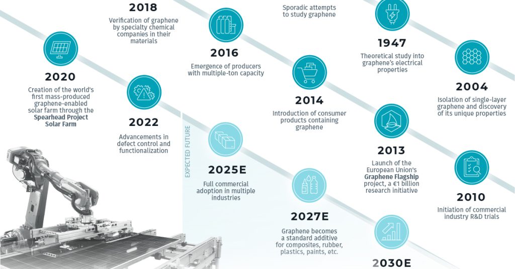
Graphene is a one-atom-thick sheet of carbon atoms arranged in a honeycomb lattice. Ever since it was first isolated in 2004 by researchers at the University of Manchester, it has awed scientists with its incredible properties and is poised to revolutionize many areas of technology.
This superlative material promises to change the landscape of the semiconductor industry and device manufacturing. But what exactly is graphene and what makes it so special? Let’s find out!
What is Graphene?
Graphene is a single layer of carbon atoms tightly packed into a 2D hexagonal lattice resembling chicken wire. It’s essentially a single atomic plane cut out of bulk graphite – the carbon material used in pencils. Graphene was presumed not to exist in the free state before 2004 as it was theorized that 2D crystals were thermodynamically unstable and would disintegrate.
However, physicists Andre Geim and Kostya Novoselov at the University of Manchester found an ingenious way to isolate and identify single-layer graphene using simple Scotch tape and microscopy techniques. For this groundbreaking discovery, they were awarded the 2010 Nobel Prize in Physics, kickstarting the graphene revolution.

Why is Graphene Amazing?
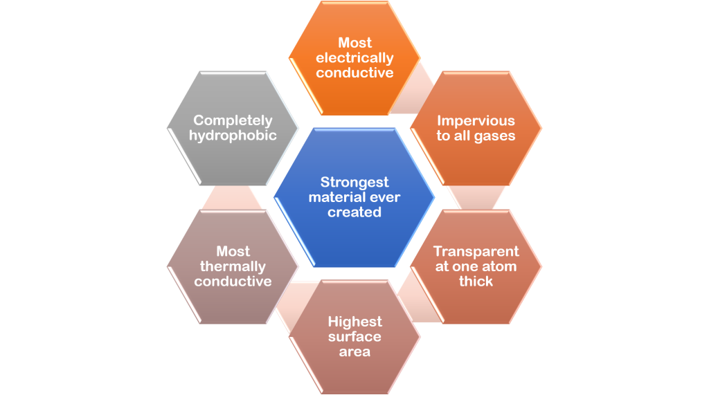
Graphene possesses a combination of spectacular properties making it enormously promising for next-generation devices:
- High Electrical Conductivity: Graphene shows exceptionally high charge mobility exceeding 200,000 cm2/Vs, even at room temperature. This allows electrons to flow freely through graphene without any scattering. Electron transport is ballistic over submicron distances indicating little electrical resistance. The conductivity also remains unchanged no matter the size or aspect ratio of the sample.
- Optical Transparency: Despite being one-atom thick, graphene absorbs just 2.3% of visible light making it almost transparent. This property combined with high conductivity makes graphene ideal for transparent electrodes in optoelectronic devices like touch screens, LEDs and solar cells.
- High Mechanical Strength: Graphene has enormous mechanical strength – one of the strongest materials ever tested. It has a breaking strength over 100 times greater than steel with a Young’s modulus of 1 TPa. It can be stretched elastically by 20% without fracture. At the same time, graphene is ultralight and just 0.77 mg of graphene covers an entire football field!
- Thermal Conductivity: Heat travels rapidly through graphene due to strong covalent sp2 bonds between carbon atoms. Graphene displays thermal conductivity higher than diamond, over 3000 W/mK. This makes it suitable for heat sinking applications in nanoelectronics.
- Chemical Inertness: Graphene surface is chemically inert owing to the complete saturation of bonding orbitals in the 2D plane. No dangling bonds or out-of-plane sites exist for participating in chemical reactions. This allows graphene to withstand extremely high temperatures without degrading.
How Does Graphene Compare to Silicon?
Silicon has been the workhorse of the semiconductor industry for over 60 years powering the microelectronics revolution, but it is facing limitations in the nano age. As per Moore’s law, electronic components are getting smaller by the year approaching the physical limits of silicon material. Graphene has emerged as the potential candidate to eventually replace or complement silicon in next-generation devices due to its vastly superior electrical, thermal and mechanical properties.
Some advantages of graphene over traditional silicon:
- Charge mobility in graphene transistors can exceed 100,000 cm2/Vs even at room temperature, nearly 100 times higher than in silicon devices. This allows switching at much higher frequencies with lower power consumption.
- Graphene remains highly conductive over a 3 times larger temperature range and demonstrates much better thermal conductivity – advantageous for device integration and heat sinking.
- The 2D nature combined with atomic thickness provides an ultimate scaling limit. Graphene transistors with 5 nm gate lengths have been demonstrated, as suitable for sub-10nm node technology.
- Mechanical strength, flexibility and chemical durability allow graphene devices on flexible plastic substrates to open door for bendable electronics.
- High optical transparency coupled with excellent conductivity makes graphene suitable for touch screens, photodetectors and photovoltaic applications.
On the other hand, graphene lacks an intrinsic bandgap which presents challenges for digital logic implementation. Creating a bandgap decreases graphene electron mobility considerably. Therefore, graphene is seen as complementing rather than replacing silicon in the semiconductor industry. While silicon will continue to dominate digital logic, graphene holds promise for next-gen high-speed analogue devices, photonic components and flexible electronics.
What Can You Do with Graphene?
Thanks to its rich set of properties, graphene promises exciting device possibilities well into the future. Here are some examples:
Faster Electronics
Graphene’s excellent conductivity, high charge carrier mobility and high current density capacity allow it to outperform copper and silver in interconnect and transistor applications. This can enable ultrafast information processing with switching frequencies reaching 1 THz!
Graphene transistors operating at 100 GHz clock rates have already been demonstrated – suitable for applications in wireless communications, imaging and radar. Biosensors made using graphene have even shown sensitivity down to detecting individual biomolecules – something previously impossible.
Flexible Touch Displays
Because graphene sheets are flexible, strong and transparent they are perfectly suited as electrode coatings for flexible touch screens in mobile phones, e-readers and tablets. Combined with other 2D crystals, graphene can enable flexible LED displays and television screens. Such graphene-based pixelated displays would be thin, light, robust and power efficient.
Prototype graphene touch screens may hit markets over the next 5 years with rollable e-paper displays following soon. Flexible OLED displays and solar cells can also leverage graphene transparent electrodes.
Energy Storage Solutions
Supercapacitors based on graphene sheets benefit from large accessible surface area of graphene flakes for charge storage. Graphene enables higher power densities for rapid charging/discharging and longer cycle lives compared to conventional supercapacitors.
When combined with manganese oxide or silicon nanoparticles, graphene nanocomposites have indicated improved performance as Li-ion battery anodes. Also, platinum nanoparticles anchored to graphene sheets have shown enhanced catalyst activity making them promising for fuel cell applications.
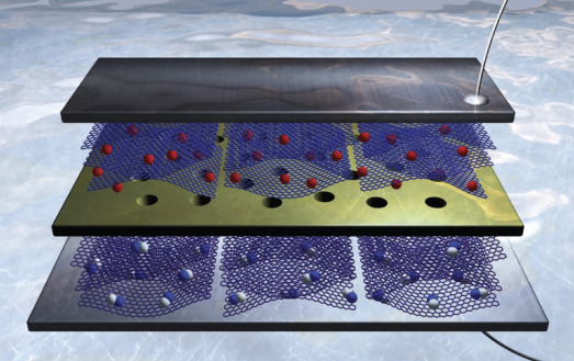
electrodes (blue and purple hexagonal planes) are separated by a membrane (yellow).
Composite Materials
Graphene flakes deliver astounding improvements in mechanical strength, electrical and thermal conductivity even when adding tiny amounts in polymer or ceramic matrices. By tuning graphene filler morphology and content, bulk composites with tailored multifunctional properties can be created.
For example, graphene-reinforced composites as structural materials are extremely light yet tougher than steel. They also display favourable electrical, thermal and barrier characteristics. Such composites are already finding use in mobile phone casings, bike frames, wind turbine blades etc but countless other applications can be envisaged.
Photonic Devices
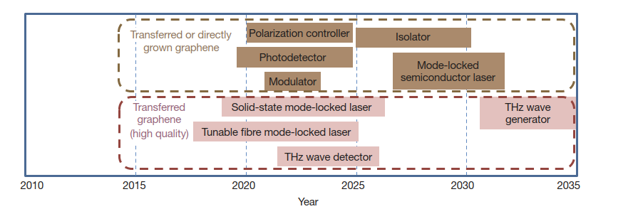
As a zero-bandgap material, graphene enables broadband light absorption and extraction across visible and infrared frequencies. This makes it promising for ultrafast photodetection from visible to THz radiation.
Thanks to the Pauli blocking principle, graphene devices can be switched from highly transparent to highly absorbing simply by applying voltage. This electro-optical switching paves the way for high-speed graphene optical modulators and tunable plasmonic metamaterials.
When combined with silicon waveguides, graphene holds the potential for on-chip optical interconnects. Shared fabrication technologies and the possibility of layer integration augurs well for future graphene photonics.
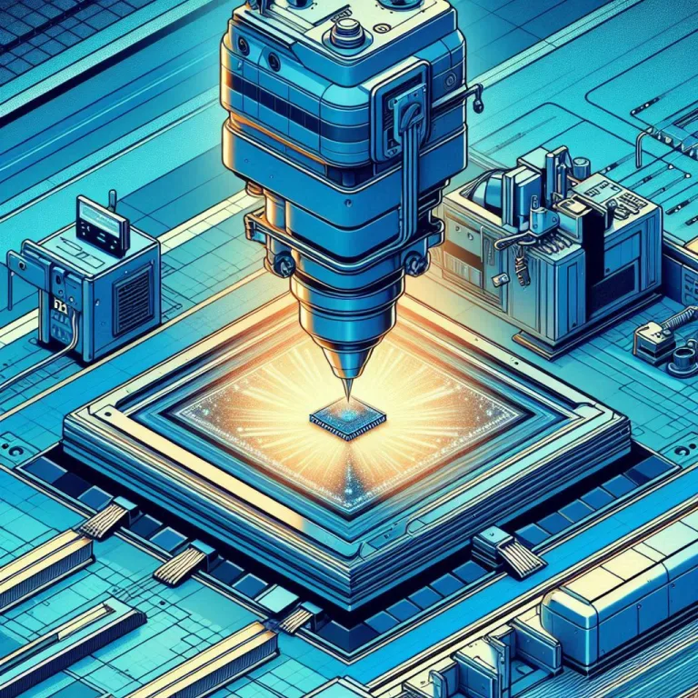
Challenges in Graphene Manufacturing
While graphene boasts an impressive array of features, realizing commercial devices brings considerable challenges. High-quality graphene with properties comparable to exfoliated flakes is still tricky to synthesize economically in large volumes. Consistent film quality, scalable production techniques and device integration need refinements before widespread graphene adoption.
Currently, CVD synthesis on copper and surface catalysis on silicon carbide are popular methods for producing graphene films over large areas. Roll-to-roll manufacturing looks promising but lowering production costs will be key to viability. Creating bandgaps without compromising on carrier mobility poses hurdles for graphene digital logic.
Environmental and health concerns surrounding graphene widths below 10 nm persist. More research is vital regarding graphene cytotoxicity and biocompatibility for enabling bioapplications. Folding graphene layers into 3D structures is also sought to further widen functional scope.
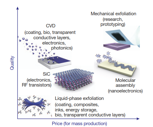
which allow a wide choice in terms of size, quality and price for any
particular application.
Future Horizons
While silicon will not disappear overnight, graphene and other 2D crystals promise an exciting materials future for a variety of niche applications, if not mass-scale electronics manufacturing outright. Within a decade, we could witness graphene adoption in transparency films, photonic components and high-frequency analogue devices. Beyond 2030, the dream of flexible graphene microprocessors might not seem so distant!
With versatile synthesis recipes, engineered bandgaps and ever-expanding application spaces from electronics and energy to composites and biomedicine, graphene’s full potential remains untapped. As material quality and large-scale production methods continue maturing, graphene is uniquely positioned to transform multiple technological domains simultaneously in the years ahead. Watch this space!
So what do you think? Will the graphene revolution change the world? Share your thoughts on this fascinating material in the comments below!