Key takeaways
- Spintronics uses the electron’s spin, and the magnetic moment that comes with it, as well as its charge.
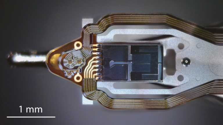
- It is already a mass-market technology: hard-disk read heads have used spin-dependent magnetoresistance, first giant and now tunnelling, since 1997, and embedded MRAM has been in commercial production since 2019.
- A magnetic tunnel junction stores a bit as the relative direction of two magnetic layers, and reads it as a resistance.
- Spin-based logic that could replace CMOS transistors is still a research goal. Spin injection into semiconductors and short room-temperature spin lifetimes are two reasons.
Electronics stores and moves information as electric charge. Spintronics adds a second property of the electron, its spin, which makes each electron a tiny magnet. Ferromagnets such as iron, cobalt and nickel conduct electrons of one spin direction more easily than the other, so a current through them becomes spin-polarised. Devices built on that asymmetry can sense magnetic fields, store bits without power, and in principle compute.

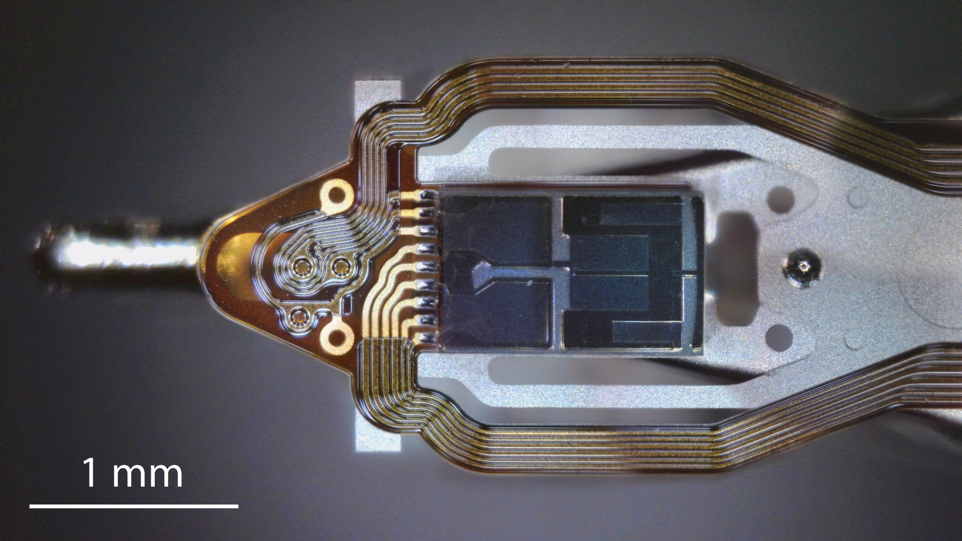
Spintronics is less futuristic than its headlines suggest. The hard drives that still hold much of the world’s stored data read their bits with spintronic sensors, and several foundries offer magnetic memory embedded next to logic. What remains open is whether spin can replace the transistor itself.
What spin is
Spin is an intrinsic angular momentum of the electron. Measured along any axis it takes one of two values, conventionally called up and down. Wolfgang Pauli introduced a “two-valued” quantum number in late 1924 to explain atomic spectra; in 1925 George Uhlenbeck and Samuel Goudsmit interpreted it as the electron spinning (Giulini, history of electron spin). A single electron can also be in a superposition of up and down, which is what spin qubits exploit, but the devices in this article use large populations of electrons and read out magnetisation as a classical bit.
The effects that make devices work
| Effect | What happens | First shown | Where it is used |
|---|---|---|---|
| Giant magnetoresistance (GMR) | Resistance of a stack of magnetic and non-magnetic metal layers depends on whether the magnetic layers point the same way | 1988, independently by Albert Fert and Peter Grünberg (Nobel Prize 2007) | Hard-disk read heads from 1997 |
| Tunnelling magnetoresistance (TMR) | Electrons tunnel through a thin insulator more easily when the magnetic layers on both sides are parallel | Large room-temperature effect from 1995; MgO barriers from 2004 | Hard-disk read heads, MRAM, magnetic sensors |
| Spin transfer torque (STT) | A spin-polarised current transfers angular momentum to a thin magnet and can flip it | Predicted by Slonczewski and by Berger in 1996 | Writing bits in STT-MRAM |
| Spin Hall effect | A charge current in a heavy metal with strong spin-orbit coupling deflects opposite spins to opposite edges, producing a pure spin current | Review: Sinova et al. 2015 | Spin-orbit torque MRAM (in development) |
| Spin Seebeck effect | A temperature gradient across a magnet drives a spin current into an adjacent metal | 2008 (Uchida et al.) | Research on spin caloritronics |

The magnetic tunnel junction
The workhorse device is the magnetic tunnel junction (MTJ): two ferromagnetic layers separated by an insulating barrier about a nanometre thick. One layer, the reference layer, has its magnetisation fixed. The other, the free layer, can point parallel or antiparallel to it. Electrons tunnel through the barrier more easily in the parallel state, so the junction has a low and a high resistance, which encode 0 and 1. The figure of merit is the TMR ratio, (RAP − RP)/RP.

Amorphous aluminium oxide barriers gave modest room-temperature ratios. Crystalline magnesium oxide barriers, demonstrated in 2004, raised them past 100%, and an MgO tunnel junction is the basis of the read head in hard drives made today (REF impact case study). The previous generation of heads, based on GMR, arrived in 1997 (Nobel Prize press release).
Get the next one by email
One new article a week on radiation, particles and the instruments that measure them, with its sources. No spam, unsubscribe any time.
MRAM: from toggle memory to embedded flash replacement
Magnetoresistive RAM stores each bit in an MTJ. The first commercial part, Freescale’s 4 Mbit MR2A16A of July 2006, wrote bits with magnetic fields from current lines and was pitched as a replacement for battery-backed SRAM (Electronic Design). Field writing scales badly, because the current needed does not shrink with the cell.
STT-MRAM writes by passing current through the junction itself, which needs far less current at small sizes. In March 2019 Samsung began mass production of embedded MRAM on its 28 nm FD-SOI process. It described write speeds about 1,000 times faster than embedded flash, because MRAM needs no erase cycle, and a module that adds few layers at the back end of the process (Samsung Newsroom).
That is MRAM’s realistic market today: non-volatile memory embedded in microcontrollers and SoCs, where flash is hard to scale, plus niche standalone parts. MRAM cells are still much larger per bit than NAND flash or DRAM, so it is not a “universal memory” for data-centre storage. Spin-orbit torque MRAM, which separates the read and write paths, is the next step under development.
What still blocks spin logic
- Spin injection into semiconductors. Injecting spin from a ferromagnetic metal straight into a semiconductor gives very low polarisation because of the conductivity mismatch between the two (Schmidt et al. 2000). A tunnel barrier at the interface is the standard workaround (Rashba 2000).
- Spin lifetime. The first electrical spin injection into silicon at room temperature measured spin lifetimes of at least 140 ps for electrons and 270 ps for holes in heavily doped silicon (Dash et al. 2009). That is enough to cross a few hundred nanometres, not a large circuit.
- Energy and speed against CMOS. Writing an MTJ still costs more energy and time than switching a transistor. Proposals such as Intel’s magnetoelectric spin-orbit (MESO) logic aim to close that gap by combining magnetoelectric switching with spin-orbit readout (Manipatruni et al. 2019).
- Materials. Ferromagnetic semiconductors that would ease integration only order well below room temperature, so practical devices rely on metallic magnets added at the back end of a CMOS process.
Where spintronics goes next
The near-term trajectory is incremental: denser embedded MRAM, spin-orbit torque cells for caches, and better magnetic sensors. Spin logic and neuromorphic circuits built from magnetic oscillators remain research topics with lab demonstrations rather than products. For readers tracking the semiconductor side of the same story, our explainer on the limits of silicon and the case for graphene covers the other main beyond-CMOS candidate.
References
- Nobel Prize in Physics 2007, press release, 9 October 2007. nobelprize.org
- D. Giulini, “Electron spin or classically non-describable two-valuedness”, 2007. arXiv:0710.3128
- M. N. Baibich et al., “Giant magnetoresistance of (001)Fe/(001)Cr magnetic superlattices”, Phys. Rev. Lett. 61, 2472 (1988). doi
- G. Binasch et al., “Enhanced magnetoresistance in layered magnetic structures with antiferromagnetic interlayer exchange”, Phys. Rev. B 39, 4828 (1989). doi
- J. S. Moodera et al., “Large magnetoresistance at room temperature in ferromagnetic thin film tunnel junctions”, Phys. Rev. Lett. 74, 3273 (1995). doi
- S. S. P. Parkin et al., “Giant tunnelling magnetoresistance at room temperature with MgO (100) tunnel barriers”, Nature Materials 3, 862 (2004). doi
- S. Yuasa et al., “Giant room-temperature magnetoresistance in single-crystal Fe/MgO/Fe magnetic tunnel junctions”, Nature Materials 3, 868 (2004). doi
- J. C. Slonczewski, “Current-driven excitation of magnetic multilayers”, J. Magn. Magn. Mater. 159, L1 (1996). doi
- L. Berger, “Emission of spin waves by a magnetic multilayer traversed by a current”, Phys. Rev. B 54, 9353 (1996). doi
- J. Sinova et al., “Spin Hall effects”, Rev. Mod. Phys. 87, 1213 (2015). doi
- K. Uchida et al., “Observation of the spin Seebeck effect”, Nature 455, 778 (2008). doi
- G. Schmidt et al., “Fundamental obstacle for electrical spin injection from a ferromagnetic metal into a diffusive semiconductor”, Phys. Rev. B 62, R4790 (2000). doi
- E. I. Rashba, “Theory of electrical spin injection: tunnel contacts as a solution of the conductivity mismatch problem”, Phys. Rev. B 62, R16267 (2000). doi
- S. P. Dash et al., “Electrical creation of spin polarization in silicon at room temperature”, Nature 462, 491 (2009). doi
- S. Manipatruni et al., “Scalable energy-efficient magnetoelectric spin-orbit logic”, Nature 565, 35 (2019). doi
- I. Žutić, J. Fabian and S. Das Sarma, “Spintronics: Fundamentals and applications”, Rev. Mod. Phys. 76, 323 (2004). doi
Cite this article
Turner, A. (2023, December 7). Spintronics Explained: GMR, MRAM and the Road to Spin Logic. ScienceShot. https://scienceshot.com/post/revolutionizing-electronics-the-rise-of-spintronics-in-semiconductor-technology
Turner, Alex. “Spintronics Explained: GMR, MRAM and the Road to Spin Logic.” ScienceShot, 7 Dec. 2023, scienceshot.com/post/revolutionizing-electronics-the-rise-of-spintronics-in-semiconductor-technology.
Turner, Alex. “Spintronics Explained: GMR, MRAM and the Road to Spin Logic.” ScienceShot, December 7, 2023. https://scienceshot.com/post/revolutionizing-electronics-the-rise-of-spintronics-in-semiconductor-technology.
@online{scienceshot-revolutionizing-electronics-the-rise-2023,
  author       = {Turner, Alex},
  title        = {{Spintronics Explained: GMR, MRAM and the Road to Spin Logic}},
  organization = {ScienceShot},
  date         = {2023-12-07},
  year         = {2023},
  url          = {https://scienceshot.com/post/revolutionizing-electronics-the-rise-of-spintronics-in-semiconductor-technology}
}
https://scienceshot.com/post/revolutionizing-electronics-the-rise-of-spintronics-in-semiconductor-technology
Get one article a week
One new article a week on radiation, particles and the instruments that measure them, with its sources. No spam, unsubscribe any time.