Key takeaways
- A CCD pixel is a small capacitor. Light frees electrons in the silicon, and a voltage on the electrode above holds them in a potential well until readout. Teledyne e2v’s CCD42-40 holds a typical 150,000 electrons per pixel.
- A CCD reads every pixel through one or a few amplifiers at the edge of the chip. Three-phase clocking shifts each charge packet down its column and then along a readout register, so the farthest pixel of a 2,048 by 2,048 chip makes about 4,096 transfers.
- A charge transfer efficiency of 0.99999 per transfer still loses 4.0% of the charge over 4,096 transfers. The CCD42-40’s typical figures (99.9999% down the columns, 99.9993% along the register) lose 1.6% over the same 4,096 transfers.
- On the CCD42-40, one electron gives 4.5 microvolts at the output and the read noise is 3 electrons rms. Between room temperature and 230 K its dark signal halves for every 5 to 8 degrees of cooling.
- Rubin Observatory’s LSST Camera, the largest digital camera ever built, uses 189 science CCD chips of 4k by 4k pixels, kept at about −100 °C.
If you looked at the first pictures from the Vera C. Rubin Observatory, released on 23 June 2025, you saw the Trifid and Lagoon nebulae as clouds of gas and dust, and a video that zooms out from two galaxies to about 10 million. In just over 10 hours of test observations, according to the release from NSF NOIRLab, the observatory recorded millions of galaxies and Milky Way stars and thousands of asteroids. The camera behind those images has 3,200 megapixels. Rubin’s own camera page compares that to roughly 260 phone camera sensors.
Your phone and that camera start the same way. Both turn light into electrons inside a thin slab of silicon. What happens to those electrons next is different. A phone camera uses a CMOS sensor. The Rubin camera records its science images on 189 charge-coupled devices, or CCDs, a design first sketched at Bell Labs in 1969.
How does a CCD turn a pattern of light into numbers, and why would a new observatory still choose it? A CCD stores the electrons where the light fell. It then moves every packet of charge, pixel by pixel, to an amplifier at the edge of the chip and measures the packets there, one at a time. On a chip of 2,048 by 2,048 pixels, the charge from the farthest corner makes about 4,096 steps before anything measures it.
Two guesses about a camera chip that do not fit a CCD
Most people picture a camera chip as millions of tiny light meters, each one read where it sits. That picture fits your phone. In a CMOS image sensor each pixel is read individually and addressed like the elements of an ordinary integrated circuit array, as the Royal Swedish Academy of Sciences describes it in its scientific background on the 2009 Nobel Prize. A CCD pixel has no amplifier of its own, so its electrons have to be carried to an amplifier at the edge.
A second guess is that the chip measures light continuously, the way a light meter shows a current. A CCD collects charge for the whole exposure and measures it afterwards. The number of electrons in each pixel is directly proportional to the light that reached it, so the pattern of stored charge is an analogue copy of the image, waiting to be read.
How light becomes a packet of electrons
The first step is the photoelectric effect, which Albert Einstein explained and which earned him the 1921 Nobel Prize. A photon (a single particle of light) that strikes the silicon can free an electron. It needs at least the band gap of silicon, 1.14 electronvolts, which is the energy that lifts an electron out of its bond in the crystal. Photons with less energy cannot free one. That puts the limit near 1,088 nanometres, in the near infrared. Teledyne e2v’s datasheet for the CCD42-40, a 2,048 by 2,048 scientific CCD, gives a spectral range of 200 to 1,060 nanometres.
Each pixel is built as a MOS capacitor, short for metal, oxide, semiconductor. A thin electrode, called a gate, sits on a layer of silicon oxide over the silicon. When the gate is given a positive voltage, it pulls the freed electrons towards it. It also pushes away the holes, the positive gaps that electrons leave behind. The electrons gather in a potential well, a dip in electric energy just under the gate where they stay put.
The silicon underneath is one continuous crystal. The pixels exist only because of the pattern of gates on top. Between the columns run strips of heavily doped silicon called channel stops, which stop charge from drifting sideways into the next column.
Not every photon is counted. Quantum efficiency is the probability that an arriving photon produces an electron. In a back-illuminated CCD the chip is thinned and lit from the back, so light does not have to pass through the gate structures first. For the back-illuminated CCD42-40 with a midband coating, Teledyne e2v specifies a minimum of 85% at 500 and 650 nanometres (green and red light), measured at −35 °C.
How much charge a pixel can hold, and where the overflow goes
A potential well can only hold so much. Full-well capacity is the number of electrons a pixel can store before its response stops following the light. For the CCD42-40 the datasheet gives a typical peak charge storage of 150,000 electrons per pixel, and at least 80,000. It defines that limit as the signal at which resolution begins to degrade.
Past that point the extra electrons spill into neighbouring pixels, which is called blooming. The channel stops block the sideways route, so the overflow runs up and down the column. Rubin’s data documentation describes the result: charge from very bright stars can overflow a pixel and extend along the column, sometimes all the way to the edge of the CCD. Astronomers call these lines bleed trails.
Some CCDs carry an anti-blooming drain, a channel next to the pixels that carries the excess charge away. The digital imaging guide from Evident, the microscope maker, gives the main drawback: lower quantum efficiency and a smaller charge capacity. Teledyne e2v builds the CCD42-40 without anti-blooming structures, its datasheet says, to improve the sensitivity. The trade is a few bleed trails around the brightest stars in exchange for more electrons from the faint ones.
The bucket brigade: moving charge with three clocks
The Academy’s background compares the readout to a bucket brigade, a line of people passing buckets of water hand to hand. Each pixel typically has three electrodes over it. Only one is needed to hold the charge, and the other two are used to move it.
Willard Boyle and George Smith set out the scheme in their first paper, in April 1970. Every third electrode is wired to the same line, so the chip has three sets of electrodes, called phases. One step works like this:
- Charge sits under electrodes 1, 4, 7 and so on, held there by their voltage.
- A stronger voltage is applied to electrodes 2, 5, 8 and so on. Their wells are deeper, so the charge flows across into them.
- The voltages change again and the charge now sits under electrodes 2, 5, 8, one position further along.
Three such steps move every packet by one pixel. In the timing used for research cameras, at least one raised barrier always separates two packets, so neighbouring pixels never mix, as lecture notes from the University of Virginia explain.
The whole image moves at once. One cycle shifts every row down by one pixel. The bottom row drops into a separate line of pixels along the edge, the serial register, which shifts its contents sideways to the amplifier, one pixel at a time. Then the image moves down another row. The Academy’s popular summary puts it simply: an array of 10 by 10 image points becomes a chain 100 points long. Because the light-sensitive pixels themselves carry the charge, a full-frame CCD such as the CCD42-40 needs a shutter to keep light out while it reads.
Why 99.999% per step is not good enough
Each transfer leaves a little charge behind. Charge transfer efficiency (CTE) is the fraction of a packet that reaches the next pixel. The Chandra X-ray Center counts the loss the same way, as the average fractional charge loss per pixel. The missing electrons are not destroyed. They trail behind and mix with the packets that follow, which smears the image along the readout direction.
Take the CCD42-40 read through one of its two amplifiers. The charge from the pixel farthest from that amplifier makes about 2,048 steps down its column and about 2,048 along the serial register, about 4,096 transfers in all. The datasheet also lists 4 extra rows and 50 underscan elements in the register, so the true count is a few dozen higher; the figures below use the round 4,096. The losses multiply, so the share that survives is the CTE raised to the power of the number of steps.
You can check it on any scientific calculator, including the one in your phone. Enter 0.99999, press the x^y key and enter 4096. The answer is 0.95987. At five nines, 4.0% of the charge from the far corner is gone before it is measured. A faint galaxy that put 1,000 electrons into that pixel arrives with 960.
The datasheet does better. Its typical figures are 99.9999% for the transfers down the columns and 99.9993% for the transfers along the register. Multiplied out, 0.9999992048 × 0.9999932048 = 0.98375, a loss of 1.6%. Most of it happens in the register: the column steps keep 99.80% and the register steps keep 98.58%. These figures count one transfer per pixel. Counted per electrode instead, with three electrodes per pixel, the same 0.99999 would leave only 88.4%.
Worked example: charge left after 4,096 transfers
| Charge transfer efficiency per transfer | Transfers | Share of charge kept | Of 1,000 electrons, arriving |
|---|---|---|---|
| 98% (the first Bell Labs devices, 1970) | 4,096 | 1.2 × 10−36 | 0 |
| 99.9% | 4,096 | 1.66% | 17 |
| 99.99% | 4,096 | 66.39% | 664 |
| 99.999% | 4,096 | 95.99% | 960 |
| CCD42-40 typical: 99.9999% down the column, 99.9993% along the register | 2,048 + 2,048 | 98.37% | 984 |
The arithmetic is the same for any chain of transfers, whether the chip sits in the Hubble Space Telescope, in an endoscope or in the Rubin camera. Space makes it worse. Charged-particle radiation damages the silicon and creates traps that hold charge back. For a dark energy space mission, Rhodes and colleagues predicted in 2010 that the resulting bias in galaxy shapes, if uncorrected, would consume the mission’s entire shape measurement error budget within about 4 years.
Get the next one by email
Power, cooling, chips and the rules that shape them. No spam, unsubscribe any time.
The output amplifier and read noise
At the end of the register each packet is tipped onto a small output node, and an amplifier turns the charge into a voltage. On the CCD42-40 one electron gives 4.5 microvolts (millionths of a volt). A full well of 150,000 electrons therefore gives 675 millivolts, the peak output voltage the datasheet lists.
Each time the amplifier reads a pixel it adds noise of its own. This is the read noise, quoted in electrons so it can be set against the signal. The CCD42-40 is specified at 3 electrons rms (the typical spread of repeated readings), and at most 4. That figure is measured at 18,000 pixels per second with a technique called correlated double sampling. With a full well of 150,000 electrons, the datasheet gives a dynamic range of 50,000 to 1. That is the span between the brightest and the faintest signal one pixel can record in a single exposure.
The low noise is measured at a slow pace. At 18,000 pixels per second, reading all 4,194,304 pixels through one amplifier takes 233 seconds, close to four minutes. Through both amplifiers it takes 116.5 seconds.
Dark current, and why the chip is kept cold
Silicon makes electrons even in total darkness. Heat alone frees some of them, and they collect in the wells together with the real signal. Boyle and Smith already named the problem in 1970: a thermally generated current that limits how long a well can hold its charge.
For the standard back-illuminated CCD42-40 at 293 K (20 °C), the typical dark signal is 20,000 electrons per pixel per second. A pixel that holds 150,000 electrons would fill itself in 7.5 seconds at room temperature, with no light at all.
The datasheet gives a formula for the range from 230 K to 300 K: Qd/Qd0 = 122 T³ e^(−6400/T), where Qd0 is the dark signal at 293 K. Worked through, it halves the dark signal for every 8.2 degrees of cooling near room temperature and for every 5.2 degrees near 230 K. At 230 K (−43 °C) it gives 24 electrons per pixel per second, 819 times less than at 20 °C. Colder still, the deep-depleted version of the chip is specified at a typical 0.2 electrons per pixel per hour at 153 K (−120 °C).
Rubin keeps its camera’s sensors at about −100 °C. Its camera page gives the reason in plain terms: the cold limits the number of defective, bright pixels in the images.
A scientific CCD and a phone sensor, figure by figure
The table puts the CCD42-40 next to a sensor built for phones: OmniVision’s 0.8 µm, 32-megapixel CMOS sensor, described by Hasegawa and colleagues at the 2019 International Image Sensor Workshop. Each figure comes from the maker’s own datasheet or paper. Conditions differ between the two, and they are stated in each cell.
| Property | Teledyne e2v CCD42-40, back-illuminated (scientific CCD) | OmniVision 0.8 µm, 32 MP CMOS sensor (phone class) |
|---|---|---|
| Pixel size | 13.5 µm square | 0.8 µm |
| Pixel count | 2,048 × 2,048 (4.19 million) | 6,528 × 4,896 (32 million) |
| Full-well capacity | 150,000 e⁻ typical, 80,000 e⁻ minimum | 5,000 e⁻ (linear full well) |
| Read noise | 3 e⁻ rms typical, 4 e⁻ maximum (18 kHz, correlated double sampling) | 1.2 e⁻ rms (16× analogue gain) |
| Dynamic range (full well ÷ read noise) | 50,000 : 1 (datasheet) | about 4,200 : 1 (calculated; combines the full well with the read noise at 16× gain) |
| Dark signal | 20,000 e⁻/pixel/s at 293 K; 0.2 e⁻/pixel/hour at 153 K (deep-depleted version) | 2.2 e⁻/s at 60 °C junction temperature |
| Quantum efficiency | at least 85% at 500 and 650 nm (midband coating, −35 °C) | published only as a normalised curve, no absolute figure |
| Charge transfer efficiency | 99.9999% parallel, 99.9993% serial (typical) | not applicable: each pixel is read through its own transistors |
| Blooming control | none: built without anti-blooming structures | blooming below 1% (measured) |
The phone pixel has the lower read noise, 1.2 electrons against 3. Per square micrometre it also stores more charge: about 7,800 electrons against about 820 for the CCD. The CCD pixel has 285 times the area, though, so it holds 30 times as many electrons in total. That gives it the wider dynamic range in a single exposure.
For how the two technologies compare as cameras, see our CCD vs CMOS comparison. For how a CMOS pixel reads itself with its own transistors, see our guide to CMOS active pixel sensors.
Where CCDs still win in 2026
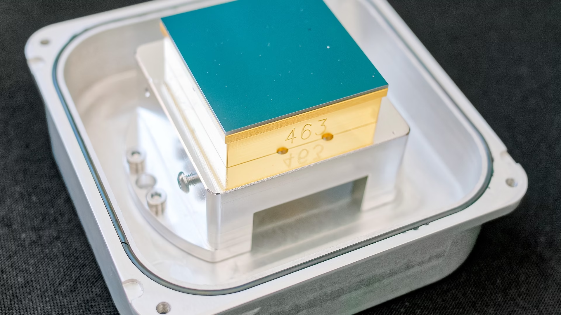
The clearest case is the one in the opening. Rubin’s key numbers page lists a focal plane of 189 science CCD chips, each 4k by 4k pixels, with pixels 10 microns across. Each pixel spans 0.2 arcseconds of sky (an arcsecond is a 3,600th of a degree). The camera was built at SLAC National Accelerator Laboratory, shipped to Chile in May 2024 and installed on the Simonyi Survey Telescope in March 2025. NOIRLab calls it the largest digital camera ever built, and each image covers an area of sky as big as 45 full Moons.
The figures in the table are the ones a survey camera of this kind needs. Rubin’s standard exposures are planned at 30 seconds, on chips kept at about −100 °C. Deep wells let bright and faint objects share one frame. A full-frame CCD also collects light over almost its entire area, close to 100% fill factor in the Academy’s words (fill factor is the share of a pixel that is sensitive to light). A Rubin pixel is 12.5 times wider than the OmniVision phone pixel, and every one of the 189 chips reads its image through the bucket brigade described above.
A memory chip sketched in under an hour
The CCD was meant to store data. Smith told the story in a 2009 review, which the Academy’s scientific background quotes. Jack Morton, the Bell Labs vice president who ran the electronics division, wanted to speed up work on magnetic bubble memory. He planned to move money from Boyle’s semiconductor division to the group working on bubbles. Morton demanded a semiconductor device that could compete. “To address this demand, on 17 October 1969, Bill and I got together in his office,” Smith wrote. “In a discussion lasting not more than an hour, the basic structure of the CCD was sketched out on the blackboard.” The Academy’s popular summary of the same prize gives September 1969 for that session instead.
The paper reached the Bell System Technical Journal on 29 January 1970 and appeared in the April issue. It describes storing charge in potential wells and moving it by moving the potential minimum. It lists possible uses as a shift register, an imaging device, a display device and in logic. In the paper that followed it in the same issue, G. F. Amelio, M. F. Tompsett and G. E. Smith reported charge transfer efficiencies above 98% for transfer times under 100 nanoseconds.
On 6 October 2009 the Royal Swedish Academy of Sciences announced that Boyle and Smith would share half of that year’s Nobel Prize in Physics, “for the invention of an imaging semiconductor circuit”. The other half went to Charles Kao, for his work on carrying light through glass fibres for communication. The 98% of 1970 was enough to prove the idea. Applied once per pixel to the 4,096 transfers of a CCD42-40 corner pixel, a generous reading of a figure measured per electrode, it would leave 1.2 × 10−36 of the charge. That is far less than one electron out of a full well of 150,000. The typical figures on the 2016 datasheet keep 98.37%.
Sources
- Royal Swedish Academy of Sciences, press release for the Nobel Prize in Physics 2009 (6 October 2009)
- Class for Physics of the Royal Swedish Academy of Sciences, Scientific Background on the Nobel Prize in Physics 2009, Two revolutionary optical technologies
- NobelPrize.org, popular information on the Nobel Prize in Physics 2009
- W. S. Boyle and G. E. Smith, Charge Coupled Semiconductor Devices, and G. F. Amelio, M. F. Tompsett and G. E. Smith, Experimental Verification of the Charge Coupled Device Concept, Bell System Technical Journal 49(4), April 1970
- Teledyne e2v, CCD42-40 NIMO back-illuminated high performance CCD sensor datasheet, A1A-100011 version 11 (November 2016)
- T. Hasegawa et al. (OmniVision), A new 0.8 µm CMOS image sensor with low RTS noise and high full well capacity, International Image Sensor Workshop 2019
- S. R. Majewski, ASTR 3130 lecture notes, Detectors: fundamentals of CCDs, University of Virginia
- Chandra X-ray Center, Pre-flight ACIS charge transfer inefficiency analysis (1999)
- J. Rhodes et al., The effects of charge transfer inefficiency (CTI) on galaxy shape measurements, Publications of the Astronomical Society of the Pacific 122 (2010) 439
- Evident, CCD blooming, digital imaging in optical microscopy
- Rubin Observatory, LSST Camera
- Rubin Observatory, Key numbers (updated 20 May 2026)
- Rubin Observatory, Data Preview 1 documentation, Image artifacts
- NSF NOIRLab, Ever-changing Universe revealed in first imagery from NSF-DOE Vera C. Rubin Observatory (23 June 2025)
Cite this article
Turner, A. (2026, October 30). How does a CCD sensor work? A pixel’s charge can travel 4,096 steps before it is read. ScienceShot. https://scienceshot.com/post/how-does-a-ccd-sensor-work
Turner, Alex. “How does a CCD sensor work? A pixel’s charge can travel 4,096 steps before it is read.” ScienceShot, 30 Oct. 2026, scienceshot.com/post/how-does-a-ccd-sensor-work.
Turner, Alex. “How does a CCD sensor work? A pixel’s charge can travel 4,096 steps before it is read.” ScienceShot, October 30, 2026. https://scienceshot.com/post/how-does-a-ccd-sensor-work.
@online{scienceshot-how-does-a-ccd-2026,
  author       = {Turner, Alex},
  title        = {{How does a CCD sensor work? A pixel’s charge can travel 4,096 steps before it is read}},
  organization = {ScienceShot},
  date         = {2026-10-30},
  year         = {2026},
  url          = {https://scienceshot.com/post/how-does-a-ccd-sensor-work}
}
https://scienceshot.com/post/how-does-a-ccd-sensor-work
Get the weekly brief
Sourced analysis of data-centre engineering and regulation, every Monday. No spam, unsubscribe any time.