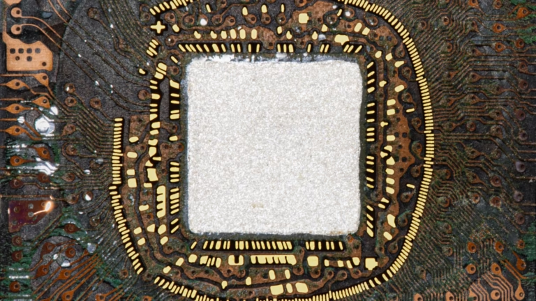
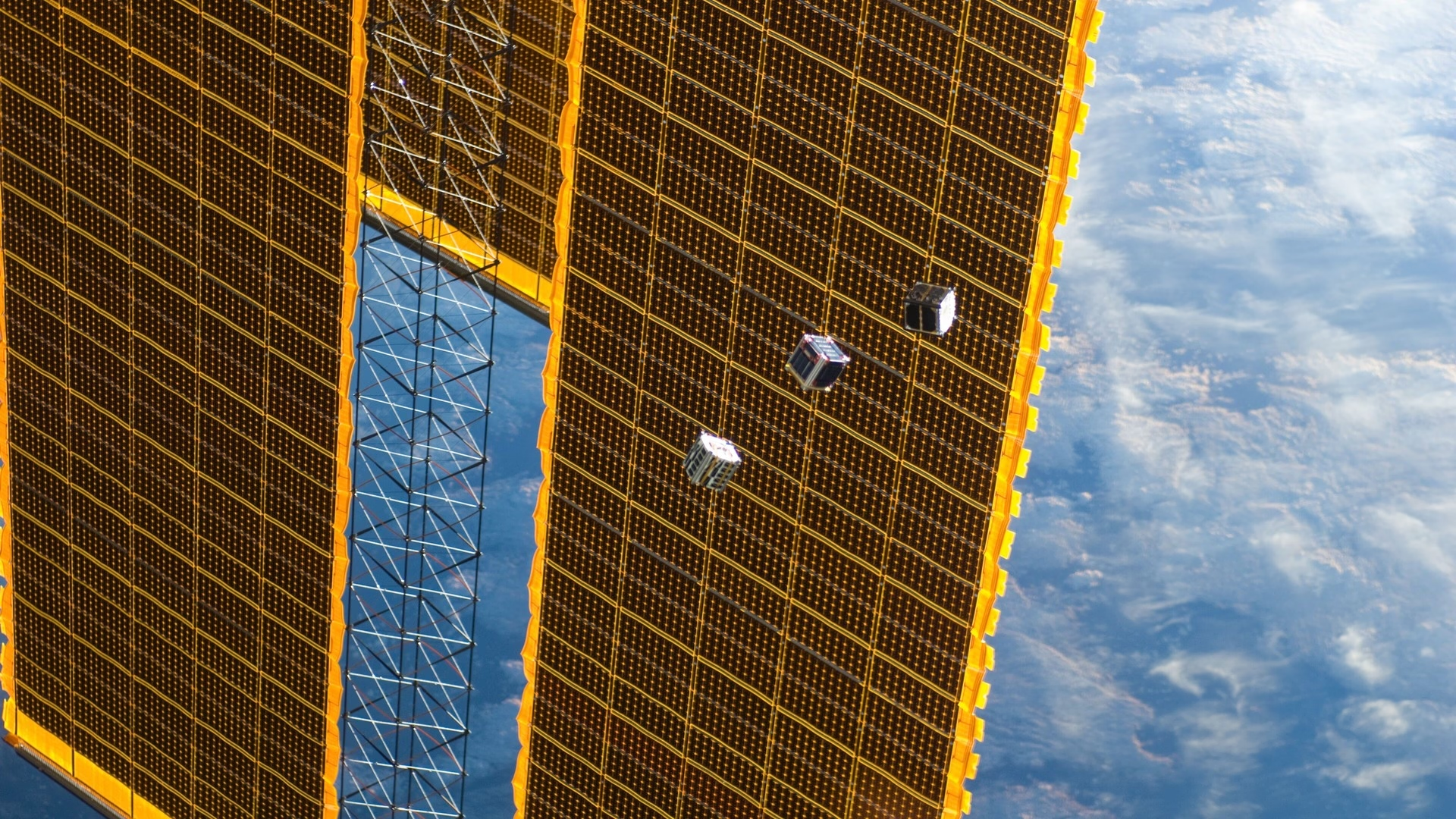
A satellite has carried an experimental radio system built with atomically thin molybdenum disulfide (MoS2) transistors. In a paper published on 28 January 2026, the researchers report that the system kept transmitting data after nine months in low Earth orbit. That is an unusually concrete result for 2D electronics. It establishes a working orbital demonstration, with a defined orbital exposure and measurement window.
What flew, and what was measured
The team made a radio-frequency system with transmitters and receivers using a wafer-scale monolayer MoS2 process. Its reported operating band was 12 to 18 GHz. The experiment flew at approximately 517 km altitude. After nine months in orbit, the paper reports a transmitted-data bit-error rate below 10-8. That figure measures communication performance in this experiment. It does not, by itself, qualify the devices for another orbit, mission life or circuit design.
The paper also estimates a much longer lifetime in geosynchronous orbit. That is a modelled projection from the authors, while the nine-month low-Earth-orbit operation is the reported flight observation. A spacecraft engineer would need the intended orbit, shielding, lifetime and failure criteria before treating either number as a part qualification.
The dose result comes from a different device
A separate 2022 study by Chen and colleagues tested few-layer MoS2 field-effect transistors with polymer solid-electrolyte gates. Those devices tolerated up to 3.75 Mrad(Si) of total ionizing dose at the study’s stated dose rate. The FETs reached a cumulative 10 Mrad(Si) across repeated irradiation and recovery cycles. Each recovery used a 100 °C, five-minute thermal anneal. These are laboratory results for that transistor architecture and recovery procedure. They are not the measured dose tolerance of the orbiting radio system.
Total ionizing dose accumulates charge-related damage over time. The dose that a spacecraft part must survive depends on its orbit or route, mission duration and shielding. Dividing Chen’s repair-assisted laboratory dose by a generic mission estimate cannot establish a material advantage over silicon. A useful comparison would test matched devices against the same radiation environment and operating conditions, including any recovery step.
Get the next one by email
Power, cooling, chips and the rules that shape them. No spam, unsubscribe any time.
Why an atomic layer is promising
An atomically thin channel may reduce the volume in which some particle interactions damage a transistor. Zhu and colleagues investigate that physical prospect alongside their system demonstration. The channel is only one part of a device: its contacts, gate dielectric, substrate and circuit nodes still affect radiation response. Comparing a monolayer channel with the full thickness of a silicon wafer says little about the relative sensitivity of finished circuits.
Space electronics must also contend with displacement damage and single-event effects. Those are distinct from cumulative total ionizing dose. This flight result shows sustained operation and a measured communication error rate under one orbital exposure; it does not establish a near-zero single-event-upset cross-section or freedom from shielding and redundancy in every design.
⚡ PHOTON’S TAKE
An operating radio in orbit is stronger evidence than a promising transistor on a bench. The next test I want to see is a matched circuit comparison under a stated radiation environment, followed by longer flight operation. Those results would tell mission designers how much of the lab advantage survives at system level.
What to watch next
The nine-month demonstration puts MoS2 radio electronics on a firmer footing. Further mission tests should report the radiation environment and accumulated dose alongside error rate, power, gain and device failures. They should also compare complete circuits with available space-qualified alternatives. Until then, the result is an experimental route to radiation-tolerant communications, with a strong orbital observation and a clear qualification gap.
Cite this article
Turner, A. (2026, August 29). MoS2 Radio Survives Nine Months in Orbit: What It Shows. ScienceShot. https://scienceshot.com/post/2d-semiconductor-radiation-tolerance-space
Turner, Alex. “MoS2 Radio Survives Nine Months in Orbit: What It Shows.” ScienceShot, 29 Aug. 2026, scienceshot.com/post/2d-semiconductor-radiation-tolerance-space.
Turner, Alex. “MoS2 Radio Survives Nine Months in Orbit: What It Shows.” ScienceShot, August 29, 2026. https://scienceshot.com/post/2d-semiconductor-radiation-tolerance-space.
@online{scienceshot-2d-semiconductor-radiation-tolerance-2026,
  author       = {Turner, Alex},
  title        = {{MoS2 Radio Survives Nine Months in Orbit: What It Shows}},
  organization = {ScienceShot},
  date         = {2026-08-29},
  year         = {2026},
  url          = {https://scienceshot.com/post/2d-semiconductor-radiation-tolerance-space}
}
https://scienceshot.com/post/2d-semiconductor-radiation-tolerance-space
Get the weekly brief
Sourced analysis of data-centre engineering and regulation, every Monday. No spam, unsubscribe any time.