Charge Carrier Generation in semiconductor materials is an important process in the development of modern electronics. It is the process by which electrons and holes are generated in a semiconductor material, allowing for current flow.
This process is essential for the operation of transistors, diodes, and other electronic components. Charge Carrier Generation is also important for the development of solar cells, as it allows for the conversion of light energy into electrical energy.
Furthermore, Charge Carrier Generation is essential for the development of optoelectronic devices, such as light-emitting diodes and laser diodes. In conclusion, Charge Carrier Generation in Semiconductor Materials is an essential process for the development of modern electronics and optoelectronic devices.
Energy Band Structure
Semiconductors are crystalline materials whose outer shell atomic levels exhibit an energy band structure, consisting of a valence band, a “forbidden” energy gap and a conduction band.
The energy bands are regions of many discrete levels which are so closely spaced that they may be considered a continuum, while the “forbidden” energy gap is a region in which there are no available energy levels at all.
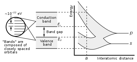
Since the Pauli principle forbids more than one electron in the same state, the degeneracy in the outer atomic shell energy levels breaks to form many discrete levels only slightly separated from each other. As two electrons of opposite spin may reside on the same level, there are as many levels as there are pairs of electrons in the crystal. This degeneracy breaking does not affect the inner atomic levels, however, which are more tightly bound.
The highest energy band is the conduction band. Electrons in this region are detached from their parent atoms and are free to roam about the entire crystal. The electrons in the valence band levels, however, are more tightly bound and remain associated with their respective lattice atoms.
The width of the gap and bands is determined by the lattice spacing between the atoms. These parameters are thus dependent on the temperature and the pressure. In conductors, the energy gap is nonexistent, while in insulators the gap is large.
At normal temperatures, the electrons in an insulator are normally all in the valence band, the thermal energy being insufficient to excite electrons across this gap. When an external electric field is applied, therefore, there is no movement of electrons through the crystal and thus no current. For a conductor, on the other hand, the absence of a gap makes it very easy for thermally excited electrons to jump into the conduction band, where they are free to move about the crystal. A current will then flow when an electric field is applied.
In a semiconductor, the energy gap is intermediate in size such that only a few electrons are excited into the conduction band by thermal energy. When an electric field is applied, therefore, a small current is observed. If the semiconductor is cooled, however, almost all the electrons will fall into the valence band and the conductivity of the semiconductor will decrease.
Charge Carriers in Semiconductors
Charge carriers in semiconductors are particles that carry electric charge through a semiconductor material. These particles are responsible for the electrical properties of semiconductors, such as their ability to conduct electricity. Charge carriers can be either electrons or holes, depending on the type of semiconductor material.
Electrons are the most common type of charge carrier in semiconductors. They are negatively charged particles that are found at the outermost energy level of the atom.
Holes are the other type of charge carrier in semiconductors. They are positively charged particles found in the atom’s innermost energy level. Holes are created when electrons move from one atom to another, leaving behind a “hole” in the atom’s energy level. Holes are responsible for the minority of electrical conduction in semiconductors.
When an electric field is applied to a semiconductor, holes and electrons are forced to move from one atom to another, creating an electric current.
At 0 K, in the lowest energy state of the semiconductor, the electrons in the valence band all participate in covalent bonding between the lattice atoms.

At normal temperatures, however, the action of thermal energy can excite a valence electron into the conduction band, leaving a hole in its original position. In this state, it is easy for a neighbouring valence electron to jump from its bond to fill the hole. This now leaves a hole in the neighbouring position. If the next neighbouring electron repeats the sequence, the hole appears to move through the crystal. Since the hole is positive relative to the sea of negative electrons in the valence band, the hole acts like a positive charge carrier, and its movement through the crystal also constitutes an electric current.
In a semiconductor, the electric current thus arises from two sources: the movement of free electrons in the conduction band and the movement of holes in the valence band. This is to be contrasted with a metal where the current is carried by electrons only.

Interaction of Particles with Matter: From Theory to Measurements
Understand the Mysteries of Radiation: Master the Interaction with Matter in a Few Simple Steps
The Energy Needed to Create Charge Carries in Semiconductors
The energy W required to create an e-h pair in a semiconductor by a charged mass particle traversing the medium depends on the band gap energy Eg of the material and hence, although only slightly, on the temperature.
The measurements of this quantity show a nearly linear dependence on the band gap energy, and the linear fit to the data obtained for different materials gives [1]

The energy for charge carrier generation is always higher than the band gap energy due to the possible additional excitation of phonon and plasmon states. Phonon excitation transfers energy to the lattice, and the energy transferred appears finally as heat in the detector.
The mean energy W to create an e-h pair has been calculated and measured in experiments including high-energy charged particles and X-ray photons [1,2]. The mean energy W required to create an e-h pair in silicon is W ≈ 3.68 eV.
References
- R.C.Alig, S.Bloom, C.W.Struck, Scattering by Ionization and Phonon Emission In Semiconductors, Phys. Rev. B, Vol.22, No.12, (1980), pp.5565-5582.
- G.W.Fraser et al., The X-ray Energy Response of Silicon, Nucl. Instr. and Meth., A 350, (1994), pp.368-378.
- S. Meroli “Interaction of radiation with matter: from the theory to the measurements”