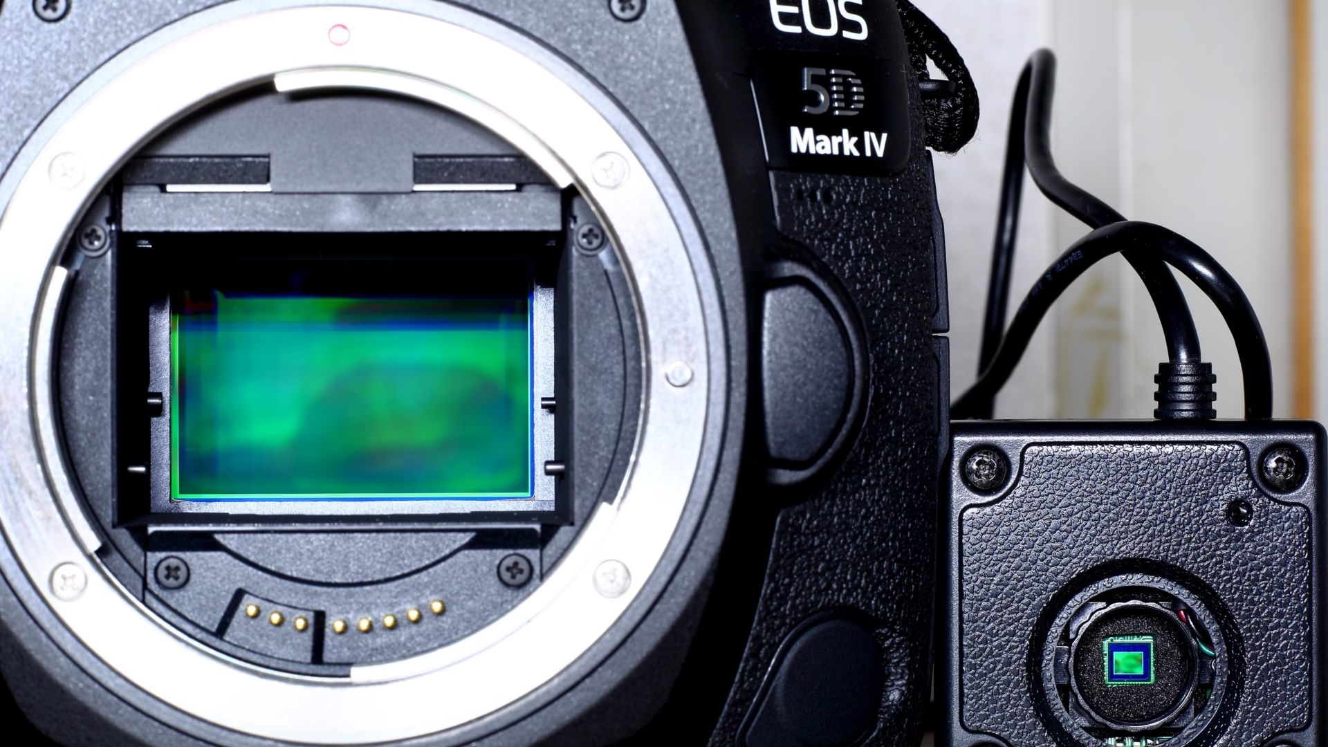
Today a scientific CMOS camera beats a good CCD on read noise and speed, while the CCD keeps the larger full well and the higher peak quantum efficiency. Datasheets read on 31 October 2026: CMOS 1.6 electrons rms at 100 frames a second; CCD 2.9 electrons at 50 kHz, 18 at 5 MHz, a visualization mode, with 4.4 frames a second.
CCD and CMOS image sensor technologies emerged in the late 1960s and early 1970s. At the time, available lithography techniques limited CMOS capability, allowing CCDs to dominate for the following 25 years. This changed a decade ago, when CMOS image sensors quickly started challenging the role of CCD sensors thanks to the following:
- Lithography and process control in CMOS fabrication had reached levels that soon would allow CMOS sensor image quality to rival that of CCDs.
- Integration of companion functions on the same die as the image sensor, creating camera-on-a-chip or system-on-a-chip capabilities.
- Lowered power consumption.
- Reduced imaging system size, as a result of integration and reduced power consumption.
- The ability to use the same CMOS production lines as mainstream logic and memory device fabrication, delivering economies of scale for CMOS imager manufacturing.
- The ability for CMOS to run on a single power source.

However, a lot has changed with CMOS and CCD technology. Some predictions turned out to be correct. Others have adapted to the changing technological environment.
Both kinds of sensors are currently supported by a thriving industry. The technological and business environments have undergone structural changes, therefore a new framework has emerged to evaluate the respective advantages and prospects of CMOS and CCD sensor technology.
CCD and CMOS in numbers
A CCD moves charge from pixel to pixel to a single output amplifier. A CMOS sensor puts an amplifier in each pixel and converts whole columns at once. That difference sets the speed and the power draw. It also explains how far the noise floor of CMOS has dropped.
| Parameter | CCD: Andor iKon-M 934 | CMOS: Hamamatsu ORCA-Flash4.0 V3 |
|---|---|---|
| Peak quantum efficiency | up to 95% (back-illuminated options) | 82% at 560 nm |
| Read noise, electrons | 2.9 at 0.05 MHz; 6.6 at 1 MHz; 11.6 at 3 MHz; 18.0 at 5 MHz (visualization mode) | 1.6 rms (1.0 median) at 100 frames/s; 1.4 rms (0.8 median) at 30 frames/s |
| Full well, electrons | 100,000 | 30,000 (typical) |
| Pixel size and array | 13 µm, 1024 × 1024 | 6.5 µm, 2048 × 2048 |
| Readout speed | 4.4 frames/s full frame, about 4.6 Mpixel/s (5 MHz) | 100 frames/s full frame, about 419 Mpixel/s (Camera Link) |
| Full well divided by read noise (derived) | 34,483 at 0.05 MHz; 5,556 at 5 MHz | 18,750 at 100 frames/s |
| Power | Moderate (qualitative, review cited below) | Low (qualitative, review cited below) |
Worked example: photoelectrons per pixel
Take a flux of 10 million photons per second per square millimetre and a one-second exposure, each camera at its peak quantum efficiency. The CCD pixel of 13 µm covers 169 µm², so it collects 1,690 photons and records 1,606 electrons. The CMOS pixel of 6.5 µm covers 42.25 µm², so it collects 423 photons and records 346 electrons.
The signal to noise ratio is S divided by the square root of S plus the read noise squared. The CCD gives 1,606 / √(1,606 + 2.9²) = 40.0 at 50 kHz and 36.6 at 5 MHz. The CMOS gives 346 / √(346 + 1.6²) = 18.5 at 100 frames a second. Neither pixel comes near its full well: 1.6% for the CCD and 1.2% for the CMOS.
At equal flux the larger pixel wins, because it collects four times the light. At very low light the read noise matters more, and the CMOS figure of 1.6 electrons is below the CCD figure of 2.9 at its slowest readout. We ignore dark current, which cooling removes in both cameras.
For the CMOS side of the story in more depth, see our guide to CMOS active pixel sensors. The same silicon senses particles as well as light. The detector signal calculator gives the electron-hole pairs a charged particle leaves in a pixel, and the materials library holds the silicon properties behind the numbers above.
Straight Path for CCDs
CCD technology has made gradual advancements in device design, materials, and fabrication technology. CCD sensors have continually enhanced quantum efficiency, decreased dark current and pixel size, reduced operating voltages (power dissipation), and improved signal handling. Furthermore, their read-out circuits have become more integrated, making CCDs easier to use and reducing time to market. CCDs now perform better with less electricity.
Get the next one by email
One new article a week on radiation, particles and the instruments that measure them, with its sources. No spam, unsubscribe any time.
The Winding Road for CMOS
Compared to CCDs, recent advancements in CMOS technology have been faster, but more turbulent. Arguably, enhancing the fill factor was the first step towards greater CMOS sensor performance. The requirement for performance and flexibility in pixel architecture competes with the quantity of space in each radiation-sensing pixel, as CMOS sensors typically require a number of optically insensitive transistors per pixel.
The pursuit of a higher fill factor and the ability to create fewer pixels has resulted in a minimum feature size of 0.5 um, which is larger than a decade earlier. CMOS sensors have progressed from fabrication process technologies of 0.35, 0.25, and 0.18 um to 90 nm in the most modern devices and, in an increasing number of cases, smaller.
Advancing lithography technology to improve fill factor and optical sensitivity boosted the possibility of digital integration on the chip since smaller transistors reduce both power dissipation and the die space required for integrated circuit operations.
However, CMOS technology’s dependence on advancing lithography came at a price. Progressively denser lithography increased development costs. And, although smaller transistor sizes facilitate digital integration, integration often increases design complexity faster than design productivity.
Substantial on-chip digital integration can bring with it noise coupling issues, with switching transients introducing noise into analogue signal pathways and even into some digital ones. Noise coupling of digital integration can conflict with the pursuit of “sensor quality”. Design complexity, design cycle duration and noise have often meant that digital integration generally has not been able to take full advantage of the lithographic trajectory of CMOS image sensors.
A more significant and unavoidable challenge of deep submicron sensor design in CMOS sensors is the analogue portion of the integrated circuit. As microelectronics fabrication technology becomes denser, analogue circuit performance typically suffers. For 0.25-um technology and smaller, supply voltages drop from 5-V levels, introducing constraints on the dynamic range at the signal levels relevant to most image sensors. Below 0.35 um, the linearity of transistor performance also tends to diminish.
Declining linearity and dynamic range combine to erode the accuracy of analogue circuitry. Other analogue performance complications, such as leakage current and complementary circuit matching issues, can arise with increasingly dense fabrication technologies.
Fighting the decline of analogue performance in deep sub-micron CMOS required a significant sensor and circuit design shift. However, because there were few relevant precedents for such high-performance digitally assisted circuit design in other applications, it has taken a number of years to develop digitally-assisted analogue architectures that fully embrace all of the competing forces among design, electro-optical performance and fabrication of CMOS image sensors.
CMOS vs. CCD Fabrication Process
The fabrication process is a defining aspect of CMOS sensor performance and has evolved considerably. From an initial notion of reusing or lightly adapting standard logic or memory processes, there has been an iterative journey to optimized CMOS pixel sensor processes.

These process technologies have often become complex in terms of the number of mask layers and process steps to meet all competing requirements. The movement of CMOS image sensors away from standard memory or logic fabrication processes started with changes to silicides and dielectrics to improve optical compatibility. Further changes have been made to:
- Reduce the optical stack height and improve its structure, thus enhancing quantum efficiency, off-axis image quality and colour fidelity.
- Introduce pixel implants and deep depletion regions to control photodiode and Si-SiO2 interface performance, influencing leakage (dark) current and image lag.
- Simultaneously manage analogue and digital transistor properties as well as interconnects.
Process optimization at each lithography node typically requires experimentation and tweaking with real reticles and silicon, not just within a simulation environment. The appreciable cost of process optimization in CMOS image sensor fabrication has shifted the advantage to manufacturers with captive foundries. Some “fab-less” players have been successful, but far more success stories have been fab-based.
It has been easier for companies with fabs to customize the fabrication process because they have been able to maintain the attention of foundry process engineers. There will continue to be viable roles for both fab-based and fab-less business models in CMOS sensor development and production. However, the original notion of easy migration of production from one CMOS fab to another has given way to a far more cohesive and adapted relationship with a particular foundry, similar to that seen in the CCD industry.
CMOS vs. CCD Technology
To reach the levels of performance needed for a variety of high-volume applications, CMOS sensor pixel design and fabrication technology now more closely resembles that of CCDs than many people had predicted. Integration and power dissipation are decisive advantages of CMOS technology, whereas CCDs retain a greater ability for cost-effective adaptation and performance. Contrary to the initial outlook, processed wafer costs have turned out to be less of an automatic advantage for CMOS.
Wafer size, economies of scale and foundry-specific cost models, however, can be bigger factors favouring one technology over the other. Regardless of wafer size, the necessity of moving to deeper submicron technology for CMOS, for fill factor and other reasons, has delivered process control and cleanliness during fabrication (compared with less advanced fabrication processes) that can improve yield, particularly for large-die-area sensors. CCD technology is not as lithography-dependent for its performance as CMOS technology.
In general, achieving application-specific performance differentiation costs less with CCD technology than with CMOS, both in sensor design and the fabrication process. CMOS has made good on its promise of integration, low power dissipation and single-voltage-supply capabilities, and intensive iterative process engineering and device design, which have led to high image quality. The production cost per unit of processed silicon does not strongly favour one technology over the other (as originally thought).
The extensive process engineering and number of fabrication steps to bring CMOS image quality to levels comparable with CCDs required much more expensive wafer processing than was originally projected. Cost is often more strongly influenced by the business economics and competitive motivations of a particular foundry than by the choice of technology itself.
There tend to be sharp differences in the wafer sizes used to manufacture CMOS and CCD image sensors, and the size depends on whether a manufacturer is fab-based or fabless and whether it is adapting a depreciated logic or memory production facility. There are more often third-party foundries available for 200-mm wafer production of CMOS image sensors, whereas CCD foundry production is frequently on 150-mm wafer lines. Captive production of CMOS and CCD is done on 150-, 200- and 300-mm lines.
A larger wafer size reduces the labour cost per unit area of silicon processed. Thus, the availability of larger wafer sizes for CCD or CMOS can be a strong factor in the overall economics of production. The cost of manufacturing one or the other also depends on the type of wafer processing available and whether downstream sensor production volumes will cover the up-front development costs.

CMOS imagers can be fabricated with more “camera” functionality on the chip. This offers advantages in size and convenience.
| Initial Prediction for CMOS | Twist | Outcome CMOS vs. CCD |
|---|---|---|
| Legacy logic and memory production lines are commonly used for CMOS image production today, but with highly adapted processes akin to CCD fabrication | Required much greater process adaptation and deeper submicron lithography than initially thought | High performance is available in both technologies today but with higher development cost in most CMOS than CCD technologies |
| On-chip circuit integration | Longer development cycles, increased cost, trade-offs with noise, flexibility during operation | Greater integration in CMOS than CCD, but companion ICs still often required with both |
| Economies of scale from using mainstream logic and memory foundries | Extensive process development and optimization required | Legacy logic and memory production lines are commonly used for CMOS imagerproduction today, but with highly adapted processes akin to CCD fabrication |
| Reduced power consumption | Steady progress for CCDs diminished the margin of improvement for CMOS | CMOS ahead of CCDs |
| Reduced imaging subsystem size | Optics, companion chips and packaging are often the dominant factors in imaging subsystem size | Comparable |
References
- D. Passeri et al., Characterization of CMOS Active Pixel Sensors for particle detection: beam test of the four sensors RAPS03 stacked system, Nucl. Instr. and Meth. A 617 (2010) 573-575
- D.Passeri,et al. Tilted CMOS Active Pixel Sensors for Particle Track Reconstruction, IEEE Nucl. Sci. Symp. Conf. Rec. NSS09 (2009) 1678. July 2006.
- L. Servoli et al. . Use of a standard CMOS imager as position detector for charged particles , Nucl. Instr. and Meth. A 215 (2011) 228-231, 10.1016/j.nuclphysbps.2011.04.016
- D. Biagetti et al. Beam test results for the RAPS03 non-epitaxial CMOS active pixel sensor, Nucl. Instr and Meth A 628 (2011) 230-233
Sources: Andor, iKon-M 934 Series specifications summary; Hamamatsu, ORCA-Flash4.0 V3 (C13440-20CU) datasheet SCAS0134E, June 2018; B. Walasek-Hoehne, K. Hoehne and R. Singh, Video Cameras used in Beam Instrumentation, CERN Accelerator School 2018, arXiv:2005.04977.
Cite this article
Turner, A. (2023, July 26). CCD vs CMOS: Which Camera Sensor Actually Takes Better Photos? ScienceShot. https://scienceshot.com/post/cmos-vs-ccd-who-is-the-clear-winner
Turner, Alex. “CCD vs CMOS: Which Camera Sensor Actually Takes Better Photos?” ScienceShot, 26 July 2023, scienceshot.com/post/cmos-vs-ccd-who-is-the-clear-winner.
Turner, Alex. “CCD vs CMOS: Which Camera Sensor Actually Takes Better Photos?” ScienceShot, July 26, 2023. https://scienceshot.com/post/cmos-vs-ccd-who-is-the-clear-winner.
@online{scienceshot-cmos-vs-ccd-who-2023,
  author       = {Turner, Alex},
  title        = {{CCD vs CMOS: Which Camera Sensor Actually Takes Better Photos?}},
  organization = {ScienceShot},
  date         = {2023-07-26},
  year         = {2023},
  url          = {https://scienceshot.com/post/cmos-vs-ccd-who-is-the-clear-winner}
}
https://scienceshot.com/post/cmos-vs-ccd-who-is-the-clear-winner
Get one article a week
One new article a week on radiation, particles and the instruments that measure them, with its sources. No spam, unsubscribe any time.