Key takeaways
- A hole is the empty state left when an electron leaves silicon’s valence band. The crystal behaves as if a particle with charge +e and a positive effective mass were moving through it.
- Peierls tied positive carriers to the anomalous Hall effect in 1929, and Heisenberg set out the hole concept for solids in 1931. The Hall coefficient of p-type silicon is positive and that of n-type silicon is negative.
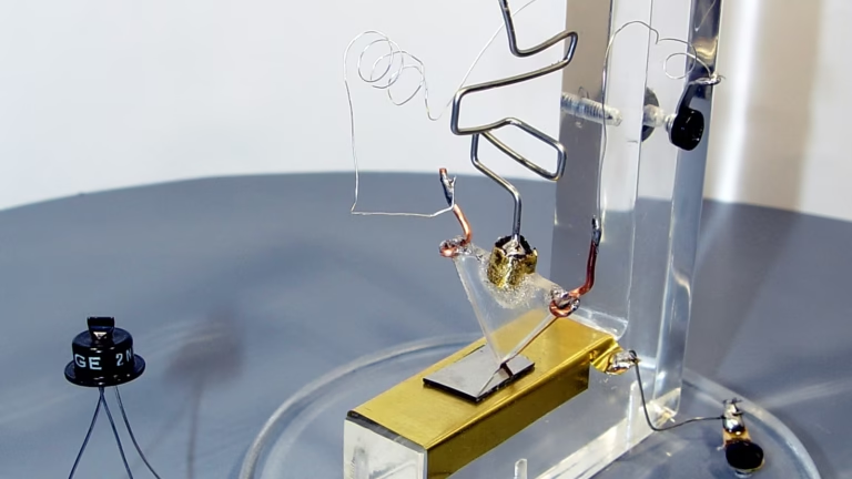
- In 1949 Haynes and Shockley reported injected holes drifting along a germanium rod. The drift speed grew in proportion to the field, and a reversed field sent no holes to the collector.
- Silicon at 300 K: hole mobility up to 450 cm²/V·s against 1,400 for electrons, a ratio of 3.1. That gap is why a PMOS transistor drives less current than an NMOS transistor of the same size.
- Silicon doped with 1016 boron atoms per cm³ has a hole mobility of about 425 cm²/V·s and a resistivity of about 1.47 Ω·cm.
What is a hole in a semiconductor? It is the empty state left in the nearly full valence band when an electron moves away. The missing electron carried a charge of minus e, so the vacancy acts like a particle of charge plus e. The curvature of the band gives that particle a positive effective mass, so it accelerates along an electric field. A hole is a quasiparticle, yet experiments measure its charge sign, mobility and diffusion constant.
Our primer on charge carriers in semiconductors introduces electrons, holes and band gaps together. This companion takes the hole alone. It covers where the idea came from, why its charge and mass carry the signs they do, and which experiments show it is real.
The band picture: what exactly is missing
At absolute zero every valence state in a silicon crystal is filled. The band gap is 1.12 eV at 300 K (Ioffe Institute database). Heat lifts a few electrons across the gap, and the intrinsic density is about 1.0×10¹⁰ per cm³. Silicon has 5×10²² atoms per cm³ (Ioffe). That is one electron-hole pair for every five trillion atoms.
Each pair leaves a vacancy behind. In the bond picture, Shockley described an electron falling into an “incomplete bond” as the removal of one hole-electron pair (Nobel lecture, 1956). The hole is a missing electron in a bond, and no atom leaves its lattice site.
A full band carries no net current. When one electron is missing, the current of the band equals what that electron would have carried, with the opposite sign. Tracking the one vacancy is far easier than tracking 1023 electrons that all shift slightly. That is the whole reason the hole is useful.
Why the hole is positive and has a positive mass
Charge comes first. Removing an electron of charge −e from a neutral crystal leaves a net +e at that spot. Peierls wrote in 1932 that the free places in a nearly full band must be given the opposite, positive charge (quoted by Hirsch, 2017).
Mass follows from the band shape. The effective mass is m* = ℏ² / (d²E/dk²), the inverse of the band curvature. Near the bottom of the conduction band the curve bends upward, so the mass is positive. Near the top of the valence band it bends downward, and electrons there have a negative mass (MIT 6.730, lecture 23).
Put the two negatives together. An electric field E pushes an electron with force −eE. Divide by a negative mass and the acceleration points along the field. The vacancy moves the same way. A particle of charge +e and positive mass |m*| would accelerate identically, which is why the MIT lecture calls the hole a quasiparticle with positive charge and positive mass.
Silicon has more than one valence band. The Ioffe database lists a heavy-hole mass of 0.49 m0, a light-hole mass of 0.16 m0 and a split-off band at 0.24 m0, where m0 is the free electron mass. The density-of-states mass that sets the carrier count is 0.81 m0 (Ioffe, band structure).
How we know it is real: the Hall effect
Edwin Hall published the effect in the American Journal of Mathematics in September 1879 (Hall, vol. 2, pp. 287 to 292). A current flows along a conductor, a magnetic field points across it, and a voltage appears sideways. The sign of that voltage follows the sign of the moving charge.
For silicon the Hall coefficient is RH = −r/(qn) for electrons and RH = +r/(qp) for holes. Here r is the Hall scattering factor. NIST used r = 0.8 for p-type silicon and r = 1 for heavily doped n-type silicon (NIST Special Publication 400-64). The two signs are opposite, so a Hall measurement tells you at once which carrier dominates.
Some metals showed a positive sign that a gas of free electrons could not explain. Peierls worked out the reason in 1929, at Heisenberg’s suggestion, using filled bands (Zeitschrift für Physik 53, 255; account in Hirsch). Heisenberg then wrote in 1931 that conduction in a metal with few holes can be described in every respect like conduction by a few positive electrons, and that the anomalous Hall effect follows directly (Annalen der Physik 402, 888).
The table dates each step from the first measurement to the textbook.
Timeline of the hole concept
| Date | Who | What | Source |
|---|---|---|---|
| Sep 1879 | Edwin Hall | Reports a sideways voltage in a current-carrying conductor placed in a magnetic field. | Am. J. Math. 2(3), 287 to 292 |
| Mar 1929 | Rudolf Peierls | Explains the positive (anomalous) Hall coefficient with band theory, at Heisenberg’s suggestion. | Z. Phys. 53, 255 to 266; Hirsch, arXiv 1704.07452 |
| 1931 | Werner Heisenberg | Introduces holes for solids and links them to the anomalous Hall effect. | Ann. Phys. 402, 888 to 904; Hirsch |
| 1932 | Rudolf Peierls | Writes that empty places in a nearly full band carry the opposite, positive charge. | Hirsch, arXiv 1704.07452 |
| 15 Feb 1949 | J. R. Haynes and William Shockley | Report hole injection in transistor action in a letter to Physical Review. | Phys. Rev. 75, 691 |
| 1950 | William Shockley | Publishes the book Electrons and Holes in Semiconductors with Van Nostrand. | Open Library record |
| 1 Mar 1951 | Haynes and Shockley | Publish the full account of the mobility and life of injected holes and electrons in germanium. | Phys. Rev. 81, 835 to 843 |
| 11 Dec 1956 | William Shockley | Describes the drift experiment in his Nobel lecture. | Nobel lecture |
Watching holes drift: the Haynes-Shockley experiment
Hall coefficients are indirect. In 1949 Haynes and Shockley reported an experiment that made holes visible in motion. Shockley described the set-up in his Nobel lecture (Nobel lecture). A germanium rod about 1/32 inch across and 1 inch long carries a sweeping field from end to end. A pulse at one point contact injects holes, and a second contact collects them downstream.
An oscilloscope records the delay between the pulse and the arrival. Doubling the distance doubles the delay. Doubling the field halves it. Reversing the field sends the holes the other way, and none reach the collector. The holes therefore move at a speed proportional to the field, as positive carriers should.
That proportionality defines mobility, v = μE. The arrival pulse also spreads out, and the spread gives the diffusion constant. The full results for germanium appeared in Physical Review 81 in 1951. Shockley gathered the theory in his 1950 book Electrons and Holes in Semiconductors. Note that the experiment used germanium. The silicon values below come from later work.
Get the next one by email
One new article a week on radiation, particles and the instruments that measure them, with its sources. No spam, unsubscribe any time.
Silicon at 300 K: electrons and holes side by side
The table gives the standard values. Intrinsic density deserves a note. Sproul and Green measured 1.00×10¹⁰ per cm³ in 1991. Altermatt and colleagues reanalysed that data in 2003 with band-gap narrowing included and obtained 9.65×10⁹. Both round to about 1010.
| Quantity | Electrons | Holes | Source |
|---|---|---|---|
| Charge | −e | +e | Bookkeeping, see above |
| Band gap | 1.12 eV | 1.12 eV | Ioffe |
| Intrinsic carrier density | 1.0×1010 cm−3 | 1.0×1010 cm−3 | Ioffe; Sproul and Green 1991; Altermatt et al. 2003 |
| Drift mobility, lightly doped | up to 1,400 cm²/V·s | up to 450 cm²/V·s | Ioffe, electrical properties |
| Diffusion coefficient | up to 36 cm²/s | up to 12 cm²/s | Ioffe, electrical properties |
| Effective mass | 0.26 m0 (conductivity) | heavy 0.49 m0, light 0.16 m0 (band masses) | Ioffe, band structure |
| Density-of-states effective mass | 1.18 m0 | 0.81 m0 | Ioffe, band structure |
| Effective density of states | Nc = 3.2×1019 cm−3 | Nv = 1.8×1019 cm−3 | Ioffe, band structure |
| Thermal velocity | 2.3×10⁵ m/s | 1.65×10⁵ m/s | Ioffe, electrical properties |
The ratio of the mobilities is 1,400 / 450 = 3.1. The diffusion coefficients follow the Einstein relation D = μkT/q. At 300 K, kT/q is 0.0259 V, so 450 gives 11.6 and 1,400 gives 36.2 cm²/s, in line with the table.
Worked example: p-type silicon doped with boron
Take silicon with 1016 boron atoms per cm³ at 300 K. Boron is an acceptor with an ionisation energy of 0.045 eV (Ioffe), so we assume every atom is ionised. Mobility falls with doping because the ions scatter carriers. The Masetti fit captures that (Masetti, Severi and Solmi, 1983). The parameters below are those listed in the Allpix Squared documentation.
| Step | Quantity | Formula and inputs | Result |
|---|---|---|---|
| 1 | Hole density | p = NA | 1.0×1016 cm−3 |
| 2 | Electron density (mass action, ni = 1.0×10¹⁰) | n = ni² / p | 1.0×104 cm−3 |
| 3 | Hole mobility, Masetti fit for boron | μp = 44.9 e−Pc/N + 470.5 / [1 + (N/2.23×1017)0.719] − 29.0 / [1 + (6.1×10²⁰/N)2], Pc = 9.23×10¹⁶ | 0.004 + 424.9 − 0.000 = 424.9 cm²/V·s |
| 4 | Conductivity | σ = q p μp = 1.602×10−19 × 1016 × 424.9 | 0.681 S/cm |
| 5 | Resistivity | ρ = 1/σ | 1.47 Ω·cm |
| 6 | Check with the upper bound of 450 cm²/V·s | ρ = 1 / (1.602×10−19 × 1016 × 450) | 1.39 Ω·cm |
| 7 | Electron contribution (μn = 1,184 from the phosphorus fit) | q n μn | 1.9×10⁻¹² S/cm, negligible |
| 8 | Same doping with phosphorus (n-type) | ρ = 1 / (q N μn), μn = 1,184 | 0.53 Ω·cm |
| 9 | Hall coefficient, r = 0.8 | RH = r / (q p) | +499 cm³/C |
| 10 | Hall voltage for I = 1 mA, B = 0.1 T, thickness 0.5 mm | VH = RH I B / t = 4.99×10⁻⁴ m³/C × 10−3 A × 0.1 T / 5×10⁻⁴ m | 0.10 mV, positive sign |
| 11 | Hole drift speed at E = 100 V/cm | v = μp E | 4.2×104 cm/s, or 425 m/s |
| 12 | Sanity check on pure silicon | ρi = 1 / [q ni (1,400 + 450)] | 3.4×10⁵ Ω·cm; Ioffe lists 3.2×10⁵ |
The result is about 1.4 to 1.5 Ω·cm, depending on which mobility you trust. The electron contribution is about three parts in a trillion of the total, so the conductivity belongs to the holes. At the same doping the n-type slice conducts 2.8 times better, because its carriers are more mobile.
Why PMOS is slower than NMOS
A transistor’s drive current at a given gate overdrive scales with the mobility of its channel carriers. In an NMOS device the carriers are electrons. In a PMOS device they are holes. In bulk silicon the mobility ratio is 3.1, and at 1016 doping the Masetti fit gives 1,184 / 425 = 2.8.
Channel mobilities in a real device differ from bulk values, so the ratio in a finished chip depends on the process. The direction never changes. EE Times noted in 2003 that designers had spent 30 years coping with the “relatively slow” holes of silicon PFETs (EE Times, 28 July 2003). The same report described Toshiba work on (110)-oriented silicon with PFET drain currents twice as fast as strained silicon on the usual (100) surface.
Holes matter beyond logic. In a silicon detector a passing particle creates electron-hole pairs, and the field sweeps the two types to opposite electrodes. Our pieces on silicon pixel sensors and CMOS active pixel sensors show where that happens. In n-type material the holes are the minority carriers, and minority carrier lifetime in silicon says how long they survive. Today’s switches built on both carrier types are covered in FinFET to nanosheet. The 1948 and 1949 work on holes also belongs to the story told in who invented the transistor.
What a hole is not
A hole is a quasiparticle, a convenient description of the many-electron crystal. It has no existence in empty space. It differs from the positron, which is a real antiparticle, and a hole cannot leave the solid. It does have a charge, a mass and a mobility that you can measure, and those measurements match the band picture.
Sources
- Ioffe Institute, NSM Archive: Basic parameters of silicon
- Ioffe Institute, NSM Archive: Band structure and carrier concentration of silicon
- Ioffe Institute, NSM Archive: Electrical properties of silicon
- P. P. Altermatt, A. Schenk, F. Geelhaar and G. Heiser, Reassessment of the intrinsic carrier density in crystalline silicon in view of band-gap narrowing, J. Appl. Phys. 93, 1598 (2003)
- A. B. Sproul and M. A. Green, Improved value for the silicon intrinsic carrier concentration from 275 to 375 K, J. Appl. Phys. 70, 846 (1991)
- E. H. Hall, On a New Action of the Magnet on Electric Currents, American Journal of Mathematics 2(3), 287 (1879)
- R. Peierls, Zur Theorie der galvanomagnetischen Effekte, Zeitschrift für Physik 53, 255 (1929)
- W. Heisenberg, Zum Paulischen Ausschließungsprinzip, Annalen der Physik 402, 888 (1931)
- J. E. Hirsch, Towards an understanding of hole superconductivity, arXiv 1704.07452 (quotes Heisenberg 1931 and Peierls 1932 and cites Peierls 1929)
- J. R. Haynes and W. Shockley, Investigation of Hole Injection in Transistor Action, Physical Review 75, 691 (1949)
- J. R. Haynes and W. Shockley, The Mobility and Life of Injected Holes and Electrons in Germanium, Physical Review 81, 835 (1951)
- William Shockley, Transistor technology evokes new physics, Nobel lecture, 11 December 1956
- Open Library, record for W. Shockley, Electrons and Holes in Semiconductors (Van Nostrand, 1950)
- MIT OpenCourseWare, 6.730 Physics for Solid State Applications, Lecture 23: Effective Mass
- G. Masetti, M. Severi and S. Solmi, Modeling of carrier mobility against carrier concentration in arsenic-, phosphorus-, and boron-doped silicon, IEEE Trans. Electron Devices 30, 764 (1983)
- Allpix Squared user manual, Charge Carrier Mobility (Masetti model parameters)
- W. R. Thurber, R. L. Mattis, Y. M. Liu and J. J. Filliben, The Relationship between Resistivity and Dopant Density for Phosphorus- and Boron-Doped Silicon, NBS Special Publication 400-64 (1981)
- D. Lammers, Toshiba designer takes path of upward mobility, EE Times, 28 July 2003
Cite this article
Turner, A. (2026, November 11). What Is a Hole in a Semiconductor? The Missing Electron. ScienceShot. https://scienceshot.com/post/what-is-a-hole-in-a-semiconductor
Turner, Alex. “What Is a Hole in a Semiconductor? The Missing Electron.” ScienceShot, 11 Nov. 2026, scienceshot.com/post/what-is-a-hole-in-a-semiconductor.
Turner, Alex. “What Is a Hole in a Semiconductor? The Missing Electron.” ScienceShot, November 11, 2026. https://scienceshot.com/post/what-is-a-hole-in-a-semiconductor.
@online{scienceshot-what-is-a-hole-2026,
  author       = {Turner, Alex},
  title        = {{What Is a Hole in a Semiconductor? The Missing Electron}},
  organization = {ScienceShot},
  date         = {2026-11-11},
  year         = {2026},
  url          = {https://scienceshot.com/post/what-is-a-hole-in-a-semiconductor}
}
https://scienceshot.com/post/what-is-a-hole-in-a-semiconductor
Get one article a week
One new article a week on radiation, particles and the instruments that measure them, with its sources. No spam, unsubscribe any time.