Key takeaways
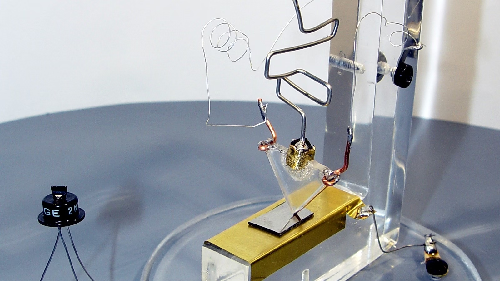
- Bardeen and Brattain built the first working transistor at Bell Labs on 16 December 1947. It was a germanium point-contact device that amplified a signal up to 100 times.
- Julius Lilienfeld filed a US patent for a field-effect transistor in 1926, granted in 1930, and Oskar Heil filed one in Britain in 1935. The Computer History Museum finds no record that either man built a working device.
- William Shockley conceived the junction transistor on 23 January 1948. That design, not the point-contact device, went into production.
- Herbert Mataré and Heinrich Welker made a point-contact amplifier in Paris in 1948 and called it the transistron. They worked independently.
- The transistor in today’s chips is the MOSFET of Mohamed Atalla and Dawon Kahng, built at Bell Labs in 1959 and shown in 1960. It is a field-effect design, the kind Lilienfeld imagined.
Who invented the transistor? John Bardeen and Walter Brattain built the first working one at Bell Labs on 16 December 1947. William Shockley then designed the junction transistor that went into products. The idea is older, since Julius Lilienfeld filed a patent for a field-effect version in 1926. The type inside modern chips, the MOSFET, came from Mohamed Atalla and Dawon Kahng in 1959 and 1960.
This piece follows the format of our dated series, which began with what Nikola Tesla invented. Each date below points to a patent, a paper or a museum record. Where the record is silent, we say so.
Transistor timeline: who did what, and when
The table runs from the first patent to a current chip. Dates are filing or event dates unless the row says otherwise.
| Date | Who | What | Source |
|---|---|---|---|
| 8 Oct 1926 | Julius Edgar Lilienfeld | Files US patent 1,745,175 for controlling current in a solid with a third electrode. Granted 28 Jan 1930, with a first priority date of 22 Oct 1925. No record shows he built a working device. | US 1,745,175, Google Patents; Computer History Museum, 1926 |
| 2 Mar 1934 | Oskar Heil | Priority date of British patent 439,457, filed 4 Mar 1935 and published 6 Dec 1935. It describes a field-effect amplifier. No record shows a working device. | GB 439,457, Google Patents; Computer History Museum, 1926 |
| Apr 1945 | William Shockley | Conceives a field-effect amplifier and switch in germanium and silicon. It fails to work as intended. | Computer History Museum, 1947 |
| 16 Dec 1947 | John Bardeen and Walter Brattain | Two gold contacts on a slab of germanium amplify a signal up to 100 times. This is the first working semiconductor amplifier. | Computer History Museum, 1947 |
| 23 Dec 1947 | Bardeen and Brattain | Demonstrate the device to Bell Labs officials. | Computer History Museum, 1947 |
| 23 Jan 1948 | William Shockley | Conceives a different design, a three-layer sandwich of n-type and p-type material, the junction transistor. | Computer History Museum, 1948 |
| 17 Jun 1948 | Bardeen and Brattain | File US patent 2,524,035, issued 3 Oct 1950. | Computer History Museum, 1947 |
| 26 Jun 1948 | William Shockley | Files US patent 2,569,347 for the junction design, issued 25 Sep 1951. | Computer History Museum, 1948 |
| 30 Jun 1948 | Bell Labs | Announces the transistor at a press conference in New York. John R. Pierce supplies the name. | Computer History Museum, 1947; PBS, John Pierce |
| Jun 1948 | Herbert Mataré and Heinrich Welker | Get consistent results from a germanium point-contact amplifier in Paris. They call it the transistron. | Computer History Museum, European invention |
| 15 Jul 1948 | Bardeen and Brattain | Publish “The Transistor, a Semi-Conductor Triode”, Physical Review 74, pp. 230 to 231. | Computer History Museum, 1947 |
| Jul 1949 | William Shockley | Publishes the theory of p-n junction transistors, Bell System Technical Journal 28 (3), pp. 435 to 489. | Computer History Museum, 1948 |
| 1956 | Shockley, Bardeen and Brattain | Share the Nobel Prize in Physics. | Nobel Prize, 1956 summary |
| 1959 to 1960 | Mohamed Atalla and Dawon Kahng | Build the first working insulated-gate field-effect transistor in silicon, the MOSFET, and announce it at a 1960 conference. | Computer History Museum, 1960; National Inventors Hall of Fame, Atalla |
| 18 Mar 2024 | NVIDIA | Announces Blackwell GPUs with 208 billion transistors. | NVIDIA press release |
So who invented it?
The answer depends on what you mean by “invent”. There are four honest answers.
The idea belongs to Julius Edgar Lilienfeld. His 1926 application describes a way to control current between two terminals of a solid by applying a third potential. It says the method suits amplifying oscillating currents “such as prevail, for example, in radio communication” (US 1,745,175). That is a field-effect transistor on paper. The Computer History Museum notes that “no records exist to prove” that Heil or Lilienfeld built a working device. Heil’s British patent of 1935 covers similar ground.
The first working device belongs to John Bardeen and Walter Brattain. Their story starts with a failure. Shockley’s field-effect amplifier of 1945 did not work, and in 1946 Bardeen suggested that electrons on the semiconductor surface were blocking the electric field. Studying those surface states led to the December 1947 device. A voltage on one gold contact modulated the current through the other.
The design that went into products belongs to William Shockley. He was not part of the December breakthrough, and the Computer History Museum says he also disagreed with Bardeen about how it worked. Within weeks he conceived the junction transistor. Its three-layer structure was easier to make reliably than two gold contacts pressed on germanium. The museum states that this is how all bipolar junction transistors work today.
The type in today’s chips belongs to Mohamed Atalla and Dawon Kahng. Their metal oxide semiconductor transistor revived the field-effect idea once they found that a layer of silicon dioxide reduced the surface states that had blocked earlier attempts. The Nobel Prize in Physics 1956 went to Shockley, Bardeen and Brattain “for their researches on semiconductors and their discovery of the transistor effect”.
Mataré and Welker deserve a place here too. Working for a Westinghouse subsidiary in Paris, they reached the same kind of point-contact amplifier in 1948. They learned of the Bell Labs news a month after getting consistent results. Thousands of their transistrons were in use in the French telephone system by mid-1949 (Computer History Museum).
Get the next one by email
One new article a week on radiation, particles and the instruments that measure them, with its sources. No spam, unsubscribe any time.
Where the name came from
John R. Pierce, a Bell Labs scientist, proposed the word. In an interview he said the transistor was meant to be the dual of the vacuum tube, which has transconductance, so it would have “transresistance”. The name also had to fit with varistor and thermistor. Accounts differ on whether the choice was made in 1948 or 1949, so the table gives only the public announcement of 30 June 1948.
From the 1947 device to the MOSFET
The point-contact transistor was delicate. Bell Labs still made many thousands of units in a metal cartridge as its Type A transistor. The junction transistor then took over because it could be made in production quantities.
Atalla and Kahng had a harder job. In 1959 they made the first successful insulated-gate field-effect transistor, with a metal gate, an oxide insulator and a silicon channel. The museum says their device was slow and addressed no pressing need of the telephone system, so Bell Labs did not pursue it. In a 1961 memo Kahng pointed to its “ease of fabrication and the possibility of application in integrated circuits”. RCA and Fairchild saw the same advantage, and MOS devices reached the market in 1964.
The museum reports that over 99 percent of microchips now use MOS transistors, because they are smaller and use less power than bipolar devices. NVIDIA announced its Blackwell GPUs on 18 March 2024 and described them as “packed with 208 billion transistors” (NVIDIA press release). One 1947 device with two gold contacts has become billions of switches on a single chip. The physical limits of those switches still matter in data centres, as our piece on cosmic rays and silent data corruption shows.
Sources
- Julius Edgar Lilienfeld, US patent 1,745,175, Method and apparatus for controlling electric currents, Google Patents
- Oskar Heil, British patent 439,457, Improvements in or relating to electrical amplifiers, Google Patents
- Computer History Museum, The Silicon Engine, 1926: Field-effect semiconductor device concepts patented
- Computer History Museum, The Silicon Engine, 1947: Invention of the point-contact transistor
- Computer History Museum, The Silicon Engine, 1948: Conception of the junction transistor
- Computer History Museum, The Silicon Engine, 1948: The European transistor invention
- Computer History Museum, The Silicon Engine, 1960: MOS transistor demonstrated
- The Nobel Prize in Physics 1956, nobelprize.org
- PBS, Transistorized!, John Pierce on naming the transistor
- National Inventors Hall of Fame, Martin (John) M. Atalla
- NVIDIA, Blackwell platform arrives to power a new era of computing, 18 March 2024
Cite this article
Turner, A. (2026, November 10). Who Invented the Transistor? A Dated Timeline. ScienceShot. https://scienceshot.com/post/who-invented-the-transistor
Turner, Alex. “Who Invented the Transistor? A Dated Timeline.” ScienceShot, 10 Nov. 2026, scienceshot.com/post/who-invented-the-transistor.
Turner, Alex. “Who Invented the Transistor? A Dated Timeline.” ScienceShot, November 10, 2026. https://scienceshot.com/post/who-invented-the-transistor.
@online{scienceshot-who-invented-the-transistor-2026,
  author       = {Turner, Alex},
  title        = {{Who Invented the Transistor? A Dated Timeline}},
  organization = {ScienceShot},
  date         = {2026-11-10},
  year         = {2026},
  url          = {https://scienceshot.com/post/who-invented-the-transistor}
}
https://scienceshot.com/post/who-invented-the-transistor
Get one article a week
One new article a week on radiation, particles and the instruments that measure them, with its sources. No spam, unsubscribe any time.